Day :
- Diamond and Carbon in biology
Location: Chicago
- Applications of graphene in energy | Carbon materials in energy | Semiconducor materials
Location: Zurich

Chair
Jong-Sung Yu
Daegu Gyeongbuk Institute of Science and Technology, Republic of Korea

Co-Chair
Rajib Paul
Case Western University, USA
Session Introduction
Jong-Sung Yu
Daegu Gyeongbuk Institute of Science and Technology, Republic of Korea
Title: Elastic nano-graphene-functionalized silicon anode for lithium ion battery with superior cycle stability and rate capability
Time : 11:05 - 11:25

Biography:
Jong-Sung Yu earned his BSc in Chemistry from Sogang University in Seoul, Korea and a PhD from the University of Houston in 1990 before Post-doctoral work at Ohio State University. He was a Professor in Korea University during 2008-2015 before he moved to DGIST. Currently, he is a Supervisor for graduate students of Light, Salts and Water Research Lab and a Chair Person at Energy Systems Engineering Department of DGIST, where his research focuses on nanostructured materials, including nanoscale 0-3D materials and their composites, and their energy applications for fuel cells, batteries, super-capacitors, sensors, and photocatalytic systems.
Abstract:
Silicon (Si), one of the most promising anode materials for next generation high-performance Li-ion batteries (LIB), is popularly studied recently because of its super high lithium capacity (4200 mAh g-1). However, Si has a dramatic volume change (~300%) during charge-discharge cycling, leading to severe capacity decay and poor cycle stability originating from its structural collapse. Carbon or graphene-modified Si is an effective method to improve its performance. Traditional three models of carbon or graphene/Si-based core-shell, yolk-shell and physical wrapping have been reported recently. However, they are still insufficient in structure to solve the silicon issues. In our work, a new concept multifunctional nano-graphene shell is elaborately designed for silicon by a low-temperature chemical vapor deposition (CVD) method on a hierarchical nickel nano-template. The as-synthesized nano-graphene-functionalized silicon (Si@NG) composite shows unique functions to challenge the current silicon anode issues in LIB. The new functional nano-graphene shell gives the full consideration of Si issues such as Si conductivity, Si volume expansion, and mass transfer, which not only can supplement poor conductivity of Si, but also self-adaptively changes their space to accommodate the lithiated Si with inflated volume by their elastic feature. More importantly, different with traditional large graphene flakes, the graphene sheets in nano size has less ions barrier effect to guarantee easy Li+ and electrolyte paths.
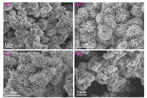
In addition, the graphene layer provides excellent protection for SEI film to guarantee high cycle stability. As an anode electrode for LIB, the Si@NG composite exhibits excellent cycling performance with high reversible specific capacity (2330 mAh g−1 at 250 mA g-1 with an initial CE of 83.4%, and 1385 mAh g−1 at 500 mA g−1 after 510 cycles with a CE of 99.2%). A superior 95% capacity retention is achieved after 510 cycles. More notably, remarkable cycling performances were obtained over harsh testing conditions of high current density and high Si@NG loading, where the Si@NG still shows several times higher capacities than commercial graphite after 1000 cycles. All the electrochemical performances get benefits from the well-designed functional graphene shells. This work demonstrates a new direction towards the development of high efficient Si anode with high capacity and super cycle stability.
Yan Song
Institute of Coal Chemistry, China
Title: Porous worm-like NiMoO4 coaxially decorated electrospun carbon nanofibers as binder-free high performance electrodes for supercapacitors and lithium-ion batteries
Time : 11:25 - 11:45

Biography:
Song Y has her expertise in preparation and application of porous carbon and energy storage materials. She is Project Leader of the National 863 project, the National Natural Science Foundation of China, key research plan of Shanxi Province, etc. She made a breakthrough in the development of preparation of high performance carbon/silicon composite anode, the pore structure control of porous nano-carbon fibers. She got several awards, such as Lu Jiaxi Young Talent Award of CAS in 2009, second prize for Science Award in Shanxi Province in 2013, first prize for National Defense Science and Technology Innovation award in Shanxi Province in 2014 and so on.
Abstract:
Recently, various nanoscale NiMoO4 structures have been synthesized and evaluated as electrode materials in both SCs and LIBs due to the relatively low cost, abundant availability, environmental benignity and inherent electrochemical advantages. Given the NiMoO4 prepared in these works exhibits small surface area and dense structure, which impedes the fast ions transport and makes it difficult to alleviate the volume change. Therefore, it will be of great significance to grow porous NiMoO4 nanostructure directly on flexible substrates for effective energy storage. As another carbon textile, electrospun carbon nano fibers (ECNFs) exhibit smaller diameter and lighter mass when compared with conventional carbon cloth, which is favorable to increase the loading of NiMoO4, shorten ion/electron transport pathways and improve the utilization of NiMoO4. The peculiar architectures consisting of electrospun carbon nanofibers coaxially decorated by porous worm-like NiMoO4 were successfully fabricated for the first time to address the poor cycling stability and inferior rate capability of state-of-the-art NiMoO4-based electrodes. The porous worm-like structure endows the electrode high capacitance/capacity due to large specific surface area and short electron/ion diffusion channels. Moreover, the robust integrated electrodes with sufficient internal spaces can self- accommodate volume variance during charge/discharge processes, which is beneficial to the structural stability and integrity. By the virtue of rational design of the architecture, the hybrid electrode delivered high specific capacitance (1088.5 F g-1 at 1 A g-1), good rate capability (860.3 F g-1 at 20 A g-1) and long lifespan (73.9% capacitance retention after 5000 cycles at 10 A g-1) when applied as supercapacitor electrode. For lithium-ion battery application, the electrode exhibited a high reversible capacity of 689.7 mAh g-1 even after 150 continuous cycles at a current density of 1 A g-1.
Shengzhong Frank Liu
Shaanxi Normal University, China
Title: Graphene-oxide doped PEDOT: PSS as a superior whole transport material for high-efficiency perovskite solar cell
Time : 11:45 - 12:05

Biography:
Shengzhong Frank Liu is currently a Professor at Shaanxi Normal University and Dalian Institute of Chemical Physics, Chinese Academy of Science. After receiving his PhD in 1992, from Northwestern University (USA), he worked in US for about 20 years in companies including United Solar, BP Solar and Argonne National Laboratory. He recently accepted Professorship in China and started to build up his research labs in Xi’an and Dalian. His research interests include nanoscale materials, thin film materials, solar energy materials, electrochemical deposition, and development of photovoltaic technologies.
Abstract:
Organometal perovskite has turned into a promising candidate material for next generation solar cells due to its high power conversion efficiency and low-cost processing. Herein we report a superior whole transport material (HTM) for significantly improved solar cell efficiency. Upon doing the commonly used PEDOT:PSS HTM by graphene oxide (GO), its hole mobility is increased from 5.55×10⁻⁵ to 1.57×10⁻⁴ cm2V-1s-1, leading to efficient hole extraction and low current leakage, therefore 20% higher power conversion efficiency comparing to the control device without the GO doping. The development open the opportunities for efficient HTMs based on the two-dimensional materials in the perovskite solar cells.
Guohua Sun
Institute of Coal Chemistry, China
Title: Porous full carbon film of graphene and activated carbon fiber for flexible supercapacitors
Time : 12:05 - 12:25

Biography:
Guohua Sun has his expertise in preparation of porous carbon materials and graphene, and application in storage components. He has developed high-performance activated carbon and graphene in a large scale, which exhibits excellent electrochemical performance for supercapacitors.
Abstract:
Binder-free and free-standing flexible carbon film with a high specific surface and bimodal porous structure was successfully prepared by a facile vacuum-assisted filtration and subsequent annealing process, in which two-dimensional graphene oxide and one-dimensional activated carbon fibres were employed as the basic building blocks.

When the mass ratio of activated carbon fiber to graphene oxide was up to 2, the as-prepared flexible film exhibited a high energy density of 20 Wh kg-1 at a power density of 11.3 kW kg-1, with a good rate capability of 63.6% retention from 1 A g-1 to 8 A g-1 and excellent capacitance retention of 94.8% after 2000 cycles in a flexible supercapacitor with 1.0 M Et4NBF4/PC as the electrolyte.
Johann Bouclé
University of Limoges, France
Title: Graphene/TiO2 composites synthesized in one-step by laser pyrolysis for improved charge extraction in perovskite solar cells
Time : 12:25 - 12:45

Biography:
Johann Bouclé is currently working as an Associate Professor at the XLIM Research Institute, University of Limoges, France, where he manages a research axis devoted to hybrid optoelectronic devices based on organic and inorganic semiconductors. After a PhD in Physics obtained in 2004, he was appointed as Post-doctoral Research Associate at Imperial College London with Prof. Jenny Nelson and then at the University of Cambridge with Prof. Neil Greenham, to develop novel hybrid solar cells based on polymers and metal oxide nanostructures. He is currently involved in the scientific boards of various French bodies in the field of printed electronics and solar cells. He is Member of the International Advisory Board of the African Graphene Center, and currently contributes to the development of graphene-based materials for photovoltaic applications, and mainly perovskite solar cells.
Abstract:
Graphene materials, including pristine graphene, graphene oxide and reduced graphene oxide, are largely explored for their outstanding electronic and optical properties, making them relevant component of optoelectronic devices such as solar cells. In this context, various solar technologies have incorporated graphene-based component (active layer, transparent or non-transparent electrodes, charge extraction layers, etc.), leading in many cases to improved power conversion efficiencies with regard to traditional materials. These developments have been rapidly transposed to highly efficient perovskite devices, which are now considered as a realistic alternative to thin film technologies, considering their easy processing from solution and the relatively high performance achieved over the last few years. In this work, we propose an original approach for the development of graphene oxide/TiO2 composites, synthesized in a single-step by laser pyrolysis, to be used as electron-extracting layer in perovskite solar cells. This method, which was successfully employed in the field of solid-state dye-sensitized solar cell incorporating TiO2/carbon nanotube composites, is based on the direct integration of a graphene suspension in the precursor mixture used for the production of anatase TiO2 particle, using an infrared laser and an aerosol precursor mixture in a cross-flow and wall-less reactor.
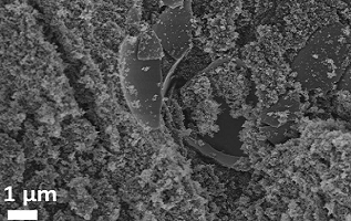
In this work, we will present the physical properties of TiO2/graphene composites by focusing on the electronic interactions between the TiO2 particles and graphene sheets using photoluminescence spectroscopy and Raman diffusion. We will also discuss the possibility to improve the charge transfer processes between the two components through the initial degree of reduction of the graphene used and the experimental conditions. Finally, we will evaluate the potentialities of the composites to demonstrate efficient selective contacts for perovskite solar cells.
Lunch Break: 12:50 - 13:30 @ Athens
Ruchi Gakhar
University of Wisconsin, USA
Title: Characterization of graphite components of FHR design
Time : 13:30 - 13:50

Biography:
Ruchi Gakhar is a Post-doctoral Research Associate at UW Madison in the Department of Nuclear Engineering and Engineering Physics. She received her PhD in Materials Science from University of Nevada, Reno in December 2015. She also holds an undergraduate and Master's degree in Chemistry and an additional Master's in Nanotechnology. During her PhD, she worked on designing of new, affordable materials to harness solar energy for clean energy production. She has published 15 journal articles and a book chapter so far. She has received several awards for academic excellence, including 2016 Nevada Regents' Scholar Award. At UW Madison, she is involved in investigating materials aspects of advanced nuclear reactor design–fluoride salt cooled high temperature reactor (FHR).
Abstract:
Two types of graphite used in the core design of Fluoride Salt Cooled High Temperature Reactor (FHR) are Graphite Matrix A3 and Nuclear Grade IG110. Matrix A3 forms the structural component for the fuel kernels, while IG110 forms the reflector blocks and some of the internal core components. Graphite forms an integral component of this design because it contributes to the structural integrity of the reactor as well as the pores of the graphite are considered as the main trapping site for the tritium produced in the coolant salt. Matrix A3 graphite which forms fuel pebble contains fission product that are produced during nuclear operation. In addition, the salt coolant or the corrosion products might intrude through the surface into the pores of the graphite. Considering these attributes, the microstructure characterization of two grades of graphite is important in developing knowledge of characteristics of graphite under FHR operating conditions. The microstructural differences between A-3 and IG-110 are attributed to the differences in the raw materials and the heat treatment temperature during manufacturing.
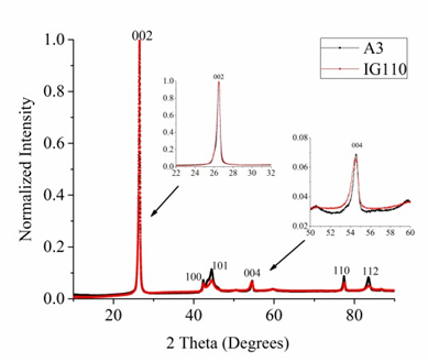
The present study focuses on the microstructure examination of two types of graphite components using X-ray Diffraction, Raman Spectroscopy, BET analysis, Mercury porosimetry and Scanning Electron Microscopy techniques. The lattice parameters, crystallite size (parallel and perpendicular to the basal plane), anisotropy and degree of graphitization estimated based on X-ray diffraction patterns and Raman spectra for both IG-110 and Matrix A3 graphite will be discussed. The similarities and differences in microstructural characteristics between the two grades of graphite as obtained using the XRD and Raman spectroscopy results will be presented and the factors causing such differences will be discussed.
Rajib Paul
Case Western Reserve University, USA
Title: Hierarchical 3D materials with vertically aligned carbon nano-structures for efficient energy applications
Time : 13:50 - 14:10

Biography:
Rajib Paul has extensive expertise in carbon material synthesis, fabrication and rational designing for efficient energy storage and conversion applications. He has developed a facile microwave radiation assisted functionalization technique for carbon based 3D porous structures. He is pioneered in nano-structuring of carbon surface through various plasma induced and thermal CVD methods. His additional research interest is related to thermal and mechanical properties evaluation in 3D hierarchical carbon structures. The foundation is based on understanding the junctional interfaces in 3D hierarchical carbon materials which play crucial roles in dictating transport and catalytic properties. He has demonstrated that the surface morphology, surface active states, and availability of carbon lattice edges evaluate the overall properties in 3D carbon structures.
Abstract:
Carbon based structural materials are attractive for energy application owing to their fascinating thermal and electrical conductivities, excellent mechanical properties and efficient catalytic activities. The sp2 hybridization in graphitic carbon lattice is responsible for such properties. The defect-free graphitic carbon structure is crucial for superior transport and mechanical properties whereas the structural or heteroatom induced defective states are desirable for efficient catalytic activities. However, the catalytic activities in defect-rich carbon materials are not always straightforward and depend on various factors, such as, type of defect, its density, surface morphology, porosity, surface area and activeness of surface defects. Furthermore, in case of hierarchically porous and three-dimensional (3D) carbon materials with abundant junctions between sp2 and sp3-hybridized carbon lattices, the understanding of catalytic and other physical properties is more difficult but important for advancement of energy storage technologies in 3 dimensions. We have opted different experimental techniques to fabricate different hierarchical carbon materials. We have grown vertically aligned few-layer graphene and carbon nanotubes (CNTs) to increase the intrinsic surface area of 3D structures. Moreover, we established an innovative technique to effectively functionalize those structures to provide active surface defects through heteroatoms (N, B) doping, for enhanced sorption based thermal energy recycling and electrochemical energy storage applications.
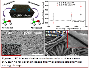
The active carbon surface demonstrated about 6-fold increase in methanol sorption enthalpy. We fabricated CNT, graphene and CNT-graphene hybrid-foams with ultra-low density (~4mg/cc) which showed ~200 % increased Li-ion storage capacity as binder-free anode. Vertically oriented CNTs grown on carbon-textiles and proper functionalization indicated high areal-capacitance of 107 mF/cm2 with excellent flexibility. We conducted experiments to understand and correlate the thermal transport and catalytic properties with structural details. The porosity is not always a dictating factor for thermal transport in 3D carbon structures rather the crystallinity and junctional properties determine the transport properties.
Ping Tang
Sichuan University, China
Title: Study on AlSb thin films prepared by pulsed laser deposition
Time : 14:10 - 14:30

Biography:
Ping Tang has her expertise in preparation and characterization of compound semiconductors and photovoltaic devices. Her research interest focuses on the study of novel compound semiconductors and related solar cells. At present, she is working on the fabrication of AlSb thin films and AlSb/ZnS based solar cells. She has succeeded in preparing AlSb thin film materials and fabricating AlSb based solar cells with architecture of TCO/ZnS/AlSb/Au and an open-circuit voltage of over 30 mV has been achieved.
Abstract:
AlSb is a kind of potential absorber material for thin film solar cells. In this paper, AlSb thin films were prepared by using pulsed laser deposition method, and the effects of substrate temperature on the properties of AlSb thin films were studied. XRD results showed that the average grain size of AlSb films increased with the increase of substrate temperature. AFM images suggested that the surface morphology of crystal AlSb thin films was continuous, homogeneous with high compactness. The electrical measurements showed that the AlSb films were semiconductors with the conductivity activation energy of 0.08, 0.17 and 0.01 eV. At the optimized temperature of 380ºc, the optical band gap of AlSb thin film was 1.52 eV. The obvious photovoltaic effect has been observed in TCO/ZnS/AlSb/Au device, which demonstrated that AlSb is a potential absorber for thin film solar cells. In present work, high quality AlSb thin films were prepared by using PLD method and the AlSb thin films we prepared were used in solar cells. The effects of substrate temperature on the properties of AlSb thin films were studied. High substrate temperature is helpful for the grain growth of AlSb films. The crystal growth was enhanced and the average grain size became larger with the increase of substrate temperature. The surface morphology of crystal AlSb thin films is continuous, homogeneous with high compactness. The electrical measurement exhibits that AlSb thin films prepared by PLD method are semiconductors with conductivity activation energy of 0.08, 0.17 and 0.01eV. The optical band gap of AlSb thin film is 1.52 eV at the optimized substrate temperature of 380ºc. Over 30 mV open circuit voltage is obtained in the TCO/ZnS/AlSb/Au device.
K Karthika
Seethalakshmi Ramaswami College, India
Title: Sonication assisted synthesis and characterization of organic and inorganic acid doped polyaniline materials
Time : 14:30 - 14:45

Biography:
K Karthika has completed her M Phil, PhD in Physics and is a UGC project fellow. Currently she is working in synthesis of conducting polymers, TiO2 and graphene based materials for energy conversion applications under the guidance of Dr. E Jasmine Vasantha Rani. She has done a project in Dye Sensitized Solar Cells by extracting natural dyes. She has published 6 papers and presented several papers in various national and international conferences.
Abstract:
In the current scenario, the conducting polymers are extensively studied due to their fascinating electronic properties and potential applications. In the present work, organic and inorganic acid doped polyaniline (PANI) salts and their dispersions were synthesized by chemical oxidative polymerization method assisted with sonication. Material characterization such as UV–Visible, FT–IR and FT–Raman were used to interpret their molecular structure, interacting nature and the effect of doping. The emission pattern of the samples was recorded through photoluminescence (PL) studies suggesting elongation of life time of charge carriers. The formation of nano fibers and nano rods were confirmed by TEM analysis. The dispersions were used as an electrolyte to measure the electrical conductivity. The electrical conductivity of the samples was found to be high due to better electron transport.
Daramola Abiodun Olamide
Walter Sisulu University, South Africa
Title: Facile synthesis of L-cysteine CdTe core shell system and its antioxidant properties
Time : 14:45 - 15:00

Biography:
Daramola Abiodun Olamide is a Material Scientist and specializes in the synthesis of nano-materials known as quantum dots. His passion is in the applicability of these materials in drug delivery system which helps in addressing some current epidemic diseases such as tuberculosis and cancer killing people every day. This has been achieved through the discovery of suitable method together with the unique optical and photo-physical properties produced by the materials. This process can successfully lead to the production of a simple drug model which can be used in our modern day society and recommended for large scale industrial purposes.
Abstract:
L-cysteine CdTe core and CdTe/CdSe core-shell were successfully synthesized in an aqueous solution medium. The synthesized QDs were analyzed using UV-vis absorption spectroscopy and florescence spectroscopy, transmission electron microscope (TEM), Fourier transform infra-red spectra (FT-IR) and X-ray powder diffraction (XRD). Systematic investigations were carried out for the determination of optimal condition namely: Reaction times, pH and mole ratios. Compared to CdTe core (529 nm), the core shell (601 nm) demonstrates a drastic shift in wavelength to the red region proving that as extra material had been deposited unto the surface of the core. The 20, 40 and 60 days stability tests conducted proved that core-shell nanoparticles were quite stable compared to the core material. Investigation was also conducted on the total anti-oxidant capacity (TAC) and lipid peroxidation with the use of six (8) Swiss albino mice and this was done using ferric reducing antioxidant power (FRAP) and TBARS was used to malondialdehyde (MDA) concentration.
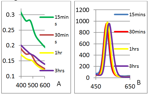
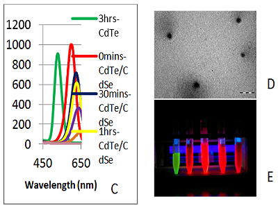
It was discovered that the core-shell demonstrated a poor anti-oxidant property at the heart, spleen, kidney and brain except at the liver where good anti-oxidant property was demonstrated after 24 and 72 hours of exposure. The result at the testis was not significant as against the control. Since this reaction did not involve the use of a nitrogen atmosphere nor special ligand or buffer solutions, it suggests that the process could be easily operated on an industrial scale.
Omotayo A Arotiba
University of Johannesburg, South Africa
Title: The application of Diamond, Graphene and Exfoliated graphite in electrochemical sensing and electrochemical degradation of organic pollutants in water

Biography:
Omotayo A. Arotiba is an Electrochemist with expertise in the applications of nanomaterials such as carbons, dendrimers, metal/metal oxides for the development of (bio)sensors and photo-electrochemical systems for biomedical, environmental (water) related problems. He is currently involved in the development of electrochemical water treatment technologies as well as sensors for toxic metals, toxins and many substances of biomedical importance. He received his BSc (Hons) and MSc in Industrial Chemistry from the University of Ilorin and the University of Benin both in Nigeria. He obtained his PhD (in 2009) from the Department of Chemistry, University of the Western Cape, South Africa. He joined the Department of Applied Chemistry, University of Johannesburg in 2010 where he is currently a Professor. He is a member of the International Society of Electrochemistry, Royal Society of Chemistry and South African Chemical institute
Abstract:
This work presents an overview of our research on the use of carbon – diamond, graphene and exfoliated graphite – in the development of electrochemical sensors and photoanodic electrodes for the electrochemical degradation of organic water pollutants. In electrochemical sensing, a novel ternary composite electrode from diamond, graphene and polyaniline was prepared, characterised and applied for the electrochemical determination of 2,4-dichlorophenol (2,4-DCP) in aqueous media. The composite, obtained via the oxidative polymerisation of aniline in the presence of graphene and diamond, was characterised by FTIR spectroscopy, Raman spectroscopy etc and used to modify a glassy carbon electrode. The electrochemical properties of the bare and modified electrodes were investigated using cyclic voltammetry, square wave voltammetry (SWV) and impedance. The determination of 2,4-DCP in 0.1 M HNO3 was carried out using SWV and a detection limit of 0.25 μM was calculated. The electrode exhibited antifouling capabilities during the electro-oxidation of 2,4-DCP. For electrochemical degradation, composites electrode consisting of exfoliated graphite (EG) and diamond were prepared and used for the electrochemical degradation of organics in water. The extent of degradation of the organics was monitored with UV/VIS spectroscopy and total organic carbon. Results showed that the incorporation of diamond into EG yielded a more robust electrode in terms of current density and also enhanced the rate of degradation of the organics. This approach is promising for the development of alternative or complementary methods for water treatment.
Marc Cretin
Université de Montpellier, France
Title: Carbon based materials: a promising approach for water depollution by electrochemical advanced oxidation processes

Biography:
Marc Cretin was born in France, in 1969. He received his Ph.D. degree in Electrochemistry (National Polytechnic Institute of Grenoble France) in 1996 and joined Geneva University to develop electrochemical sensors for biomedical and environmental analysis. In 1998 he gained a position of assistant professor (ENSCM/Montpellier/France) to work on membranes materials for detection, separation and reaction. He’s full professor since 2012 at the University of Montpellier and works mainly in the field of materials for energy and environment. He focuses his research mainly on electroactive materials for fuel cells, biofuel cells, EAOP (electrochemical advanced oxidation processes) and ceramic membranes for water treatment. He’s currently Director of the department “Physico-Chemistry, Interface and Polymer” at the European Membrane Institute of Montpellier (IEM) and co-director of the International French-Russia Laboratory MEIPA “Ion Exchange Membranes and Associated Processes”. Up to March 2017, he has co-authored more than 80 peer reviewed papers.
Abstract:
Gustavo Lopez Velazquez
Universidad de Guadalajara, Mexico
Title: Cuantum computation in a solid state diamond C12 with a chain of C13 atoms

Biography:
Abstract:
Somnath Bhattacharya
University of the Witwatersrand, South Africa
Title: Quantum device prospects of superconducting diamond films

Biography:
Somnath Bhattacharyya is a Professor in the School of Physics at the University of the Witwatersrand, Johannesburg, South Africa focusing on the area of condensed matter physics and nano-electronics. His major interest is in the transport properties of carbon and major achievements include the demonstration of resonant tunnel devices based on amorphous carbon, gigahertz transport in carbon devices, n-type doping of nanocrystalline diamond and developing theoretical models for transport in disordered carbon. His team focuses on the fabrication of the nanoelectronic devices, studying novel electronic properties of nanocrystalline diamond films and carbon superlattice structures at high magnetic fields and high frequencies. His group is also involved in performing theoretical modeling of carbon quantum structures. He is engaged in developing a new infrastructure for a wider range of nanotechnology that will include quantum matter, carbon based microwave detectors and nano-bio-electronics.
Abstract:
Nanostructured semiconducting carbon system, described by as a superlattice-like structure demonstrated its potential in switching device applications based on the quantum tunneling through the insulating carbon layer [1-4]. This switching property can be enhanced further with the association of Josephson’s tunneling between two superconducting carbon (diamond) grains separated by a very thin layer of carbon which holds the structure of the film firmly [5]. The superconducting nanodiamond heterostructures form qubits which can lead to the development of quantum computers provided the effect of disorder present in these structure can be firmly understood. Presently we concentrate on electrical transport properties of heavily boron–doped nanocrystalline diamond films around the superconducting transition temperature measured as a function of magnetic fields and the applied bias current. We demonstrate signature of anomalous negative Hall resistance in these films close to the superconductor-insulator-normal phase transition at low bias currents at zero magnetic field [5]. Current vs. voltage characteristics show signature of Josephson-like behavior which can give rise to a characteristic frequency of several hundred of gigahertz. Signature of spin flipping also shows novel spintronic device applications. We are working towards utilizing the superconducting phenomena in nanodiamond films in making some novel quantum electronic and high speed devices. This project complements our previous work on nitrogen-doped nanodiamond films and related nanostructured carbon devices which showed interesting radio frequency features in the gigahertz range [6].
- Graphene modification and functionalization | Nano carbon materials | Applications of graphene in biomedical
Location: Zurich

Chair
Adam Khan
AKHAN Semiconductor, Inc., USA
Co-Chair
Yung Woo Park
Seoul National University, South Korea
Session Introduction
Guang Li
Donghua University, China
Title: The control of pore sizes in porous carbon fiber and its enhanced microwave absorption

Biography:
Dr. Guang Li received her M.Sc in Chemistry from China Textile University in 1985, and her Ph.D in material science and engineering from Donghua University in 2006. She was a Senior Visiting Scholar in the University of Twente (Netherlands). She has been a full Professor at Donghua University sine 1999, and continuously working on high performance polymer , porous carbon fibers and their associated processing and applications. She has published more than 100 scientific papers in high-impacting peer-reviewed journals and has given more than 24 keynote/invited/oral presentations, co-authored 4 books, and owns 26 patents. Dr. Li has been awarded several prizes for recognizing her contributions to science and technology.
Abstract:
As one of carbon materials, the porous carbon fiber has played a great role as catalyst support, separation by absorption, gas storage etc. based its high aspect ratio. Among related publications, few studies focused on the microwave absorption characteristics of porous carbon fibers, although a great number of papers concerned carbon materials such as carbon black, fiber, tube as microwave absorbents[1-3]. In this study, Porous carbon fibers were prepared through carbonization of the blend fibers composed of poly(acrylonitrile) (PAN) and poly(methyl methacrylate) (PMMA)with 70 wt % of PAN. The pore size in porous carbon fibers could be controlled by changing the average molecular weight of PAN, The pores of 1-10μm and 0.1-1μm in diameter were obtained from the blend fibers where the average molecular weight of PAN is 51000 and 83000 g/mol, respectively(Figure 1). The obtained porous carbon fibers were used as absorbents to make epoxy composites with addition of 2-6 wt %. The microwave absorption properties were stimulated based on a model for a single-layer plane wave absorber. The results explained the porous carbon fiber showed much better microwave absorption than carbon nanofiber, and the porous carbon fiber with small size of pores showed much better microwave absorption than that with large size of pores, as shown in figure 2. It is believed that the enhanced microwave absorption from the porous carbon fibers is due to a combination of the dielectric-type absorption and the interference of multi-reflected microwaves[3-6]. When the pore size in porous carbon fibers is large, the air-absorber interfaces could be reduced at the same pore volume. Therefore, the superior microwave absorption of composites filled by porous carbon fiber with smaller pore size may be ascribed to the combination of absorption and interference of microwaves.
Anirudha V Sumant
Center for Nanoscale Materials, Argonne, National Laboratory,USA
Title: Towards developing energy efficient systems based on novel carbon materials

Biography:
Anirudha Sumant is a Materials Scientist working at Center for Nanoscale Materials, Argonne National leading the research on nanocarbon materials including CVD-diamond, carbon nanotube and graphene. He has more than 22 years of research experience in the synthesis, characterization and developing applications of carbon based materials. His main research interests include electronic, mechanical and tribological properties of carbon based materials, surface chemistry, micro/ nano-scale tribology, and micro-nanofabrication. He is the author and co-author of more than 100 peer reviewed journal publications, 2 book chapters, winner of four R&D 100 awards, NASA Tech Brief Magazine Award, 2016 TechConnect National Innovation Award, has 16 patents granted, and 15 pending and given numerous invited talks. His research in diamond materials helped in the formation of several start-up companies including NCD Technologies Inc. and AKHAN Semiconductors Inc. He is a member of MRS, STLE and AVS.
Abstract:
Minimizing friction and wear-related mechanical failures remains as one of the greatest challenges in today’s moving mechanical systems leading to a search for new materials that can reduce friction and wear related energy losses and the understanding of fundamental mechanisms that control friction. In this context, our work on graphene has shown that this materials properties can be manipulated at the atomic level to achieve exceptionally high wear resistance, as well as well as achievement of superlubricity (or near zero friction) at macroscale through combined use of graphene and nanodiamonds on sliding surfaces [1]. This discovery presents a paradigm shift in understanding frictional behavior of graphene and other 2D materials and offers a direct pathway for designing energy efficient frictionless tribological systems. In the second part of my talk, I’ll describe our recent work on direct growth of wafer-scale graphene on diamond. The fact that the one atom thick graphene membrane strongly affected by the substrate interactions puts limit on exploiting excellent intrinsic properties of graphene for various applications. Diamond offers multiple unique properties, such as high phonon energy, low trap density, and high thermal conductivity, which make it an ideal substrate for fabricating graphene devices on diamond [2]. We demonstrate a novel process to grow large area single and few layer graphene directly on the diamond thin film deposited on silicon wafer thus eliminating the need for graphene transfer [3]. This approach offers new opportunities for developing graphene based nanoelectronic devices directly on dielectric substrate (diamond/Si) and provides reliable, efficient and low cost alternative as compare to current methods.
Yung Woo Park
Seoul National University, Korea
Title: Manipulation of electrical properties in CVD-grown twisted bilayer graphene induced by dissociative hydrogen adsorption
Time : 15:00 - 15:20

Biography:
Y W Park graduated summa cum laude in 1975 from the Physics Department of Seoul National University in South Korea. He received his PhD from University of Pennsylvania, Philadelphia, United States in 1980. His PhD thesis on the "Electrical Transport Studies of Pure and Doped Polyacetylene" was supervised by Professor Alan J Heeger. He was involved in the original discovery of conducting polymers in 1977 under the guidance of Prof. Alan J Heeger. He has made unique contributions on the synthesis and transport studies of carbon based nanostructures such as conducting polymer nanofibers, carbon nanotube, organic conductors, molecular conductors and graphene. He has also contributed significantly to the transport and mechanism studies of highly correlated materials, such as high Tc superconductors. In particular, his recent discovery of "Zero magneto resistance in polymer nanofibers" is his most important and seminal achievement. In particular, the CNT based nonvolatile MEMS memory has achieved a 1000 times faster switching speed, applicable to the MP3s, smart phones and cameras with very low power consumption and possible multinary bit devices
Abstract:
The effect of hydrogen adsorption on twisted bilayer graphene (tBLG) was studied. Raman spectroscopy and the electrical transport properties (electrical resistance and thermoelectric power) confirm that the electron doping by hydrogen adsorption, in agreement with the previous report involving exfoliated bilayer graphene (BLG). Common electron doping behavior were observed at various twist angles (0o, 5o, 12.5o and 30o), and the adsorptions follow the first–order Langmuir-type adsorption model. Specifically, we analyzed the off-state currents, with band-gap openings of around 13 meV in tBLG with twist angle of 0o, as in Bernal-stacked BLG.
Adam Khan
AKHAN Semiconductors, Inc., USA
Title: Thin film nanocrystalline diamond for optical and monolithically integrated display applications
Time : 15:20 - 15:40

Biography:
Adam Khan is the Founder and CEO of AKHAN Semiconductor. He is currently leading the technology development program. His research interests include theoretical work in unconventional superconductor systems and applied work in n-type diamond semiconductor systems. He is listed inventor to over 11 issued and pending patents and has authored several published technical works in addition to roles like co-chairing technical conferences and symposia. He is also the winner of a 2013 R&D 100 award, Clean Tech Open Midwest Innovation Summit winner, and 2014 Forbes 30, under 30 in Energy and Industry. He earned his BS in Electrical Engineering and Physics from the University of Illinois Chicago, before pursuing graduate research at Stanford University’s Stanford Nanofabrication Facility.
Abstract:
Diamond is well-known for its extreme hardness, high- optical transparency, high thermal conductivity, and great chemical stability. In spite of all these excellent properties, diamond has largely been absent in optical applications due to the difficulty in fabricating high quality diamond thin films at lower substrate temperatures cost efficiently. Pioneering work on low temperature, high quality diamond deposition methods by AKHAN semiconductor Inc. has opened doors for the use of diamond in a wide variety of optical applications. Nanocrystalline diamond (NCD) coatings with grain size of 10-100 nm can significantly enhance the breakage, scratch performance and hydrophobicity of glass displays and lenses. In this work, NCD thin films of 50-250 nm thickness were deposited on commercial BK7 glass and chemically hardened aluminosilicate glass (Gorilla Glass) substrates using hot filament and microwave plasma chemical vapor deposition (HFCVD and MWCVD) techniques under optimized substrate temperatures to avoid substrate deformation.
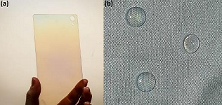
Optical characterization work of the as deposited NCD films was performed using ellipsometry, spectral reflectance and spectrophotometry over visible wavelengths. Mechanical characterization work was also performed to obtain hardness and young’s modulus data for the NCD films. Measured results demonstrate the viability of NCD as a protective coating for a broad range of optical applications. Additionally, low temperature, high quality diamond deposition allows complementary metal oxide semiconductor (CMOS) device integration on optical substrates opening new opportunities for the development of next-generation monolithically integrated transparent devices and electronics.
Zahra Sadeghian
Research Institute of Petroleum Industry, Iran
Title: Superhydrophilic functionalized graphene oxide-ceramic composite membrane for enhanced oily produced water treatment
Time : 15:40 - 16:00

Biography:
Zahra Sadeghian is Associate Professor of Materials Science and Engineering. She has received PhD from TU Clausal, Germany in 2005. She has done Post-doctoral Fellowship in Chemical Engineering (membrane process) at RWTH Aachen University in 2010. She is working at Research Institute of Petroleum Industry from 2005. Her expertise is in nanostructured coatings for surface modification and nanomaterial synthesis such as carbon nanotube and graphene and their composites. Also, she has been investigating on ceramic composites in adsorbent, biomaterials, catalysts and membranes applications. She has experiences in oilfield produced wastewater treatment and desalination pilot plant using ceramic membranes and their composites. She has been fabricating ceramic membranes for separation of hydrogen from syngas and other gases.
Abstract:
The largest wastewater stream is generated in oil and gas industries. In order to meet environmental regulations as well as reuse and recycling of produced water, treating oily produced water is very important. In this research, nanofiltration (NF) membranes with functionalized graphene oxide (F-GO) for wastewater treatment have been worked on. In this work, the synthesized GO from our previous work (Fig. 1a) was first functionalized with polyethyleneimine (PEI). The PEI–GO thin film has been constructed on home-made microporous γ-alumina/alumina substrate to enhance and improve the characteristics of nanofiltration (NF) alumina membranes. Fig. 1b shows microstructure of ceramic membrane surface modified PEI-functionalized GO representing compressed thin layers. The interactions between PEI–GO and the alumina matrix are caused to make passageways for water rapidly passing through membrane. Also the contact angle and zeta potential results showed a notable increase in surface hydrophilicity of the thin layers accompanying presence of positively charged PEI. The filtration properties of the membrane were tested by home-made cross flow NF using oily wastewater with oil concentration of feed 5000 mg/L. High oil (>99%) and total organic carbon (TOC) rejection (>99%) was obtained using the prepared membrane.
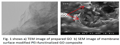
Also the water flux was almost 10 times higher than that of the pristine alumina membrane. The permeation flux-decline is decreased to an ultralow level (less than 1%) that it turns to the antifouling layers on modified membrane surface. The superior antifouling property is mainly focused on surface structure of the membrane such as superhydrophilic character and charge of the modified alumina surface. As a result, the PEI–GO/alumina hybrid membrane showed an effective method for preparing composite NF membranes with effective reinforced permeation and superior antifouling property that it improves the performance of the oil separation and wastewater treatment.
Coffee Break: 16:05 -16:25 @ Foyer
Pedro Alpium
International Iberian Nanotechnology Laboratory, Portugal
Title: Graphene functionalized field-effect transistors for biomedical applications
Time : 16:25 - 16:45

Biography:
P Alpuim is the Group Leader in 2D materials and devices at INL. He works in 2D materials CVD and device fabrication, with emphasis in biosensors. Optoelectronic devices for light detection and solar energy conversion are within his research interests. He is a Professor in the Physics Department of the University of Minho (UM), where he teaches graduate and undergraduate courses on the physics of electronic devices, nanotechnology, and clean-room fabrication. He received a PhD degree in Materials Engineering from IST Lisbon in 2003, working in silicon thin film devices for flexible electronics, and a Master’s degree in Physics from the UM in 1995. He installed a thin-film laboratory at UM where he focused on fabrication of thin-film silicon solar cells, piezo resistive sensor arrays for health care and thermoelectric junctions of telluride compounds for micro-cooling and energy scavenging.
Abstract:
The importance of bio sensing systems in biomedical research is steadily increasing, as they became pervasive in a large range of health applications, from prognosis and diagnosis to personalized medicine. Graphene is a material of choice for sensing applications, with its highly conjugated, high mobility, zero bandgap 2D electronic system providing extreme sensitivity to charges and electric fields in its vicinity, combined with a high chemical stability and ease of processing. However, specific target biorecognition on graphene requires surface functionalization. We developed a general process for immobilization of probe molecules on graphene surfaces, based on π-π interactions with a pyrenic linker (PBSE). Electrolyte-gated field-effect transistors (FETs), with receded integrated gate architecture were fabricated at the 200 mm wafer scale followed by functionalization of the graphene channel for detection of antigens and DNA.
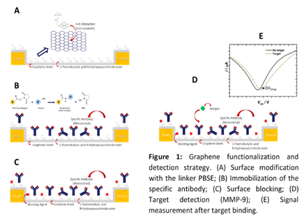
A graphene immuno-FET is designed to detect the biomarkers of the hemorrhagic transformation of ischemic stroke. The probe is immobilized by reaction of the PBSE succinimidyl ester groups with a primary amine from the antibody protein. The device is able to detect the biomarker (MMP-9) in concentrations down to 0.01 ng/mL, in a range up to 10 ng/mL. Compared with existing MMP-9 immunoassays, ours has a much shorter time to diagnostic since it is based on a simpler label-free protocol. The nucleic acid sensor is made by immobilization of single-stranded DNA (25 nucleotides long) on the PBSE-functionalized graphene transistor channel. Hybridization with complementary DNA was detected down to 1 aM, with a saturation attained at 100 fM and sensitivity to single nucleotide polymorphism. These results show that the fabrication of graphene sensors using standard clean-room technology, with high sensitivity and low cost, is possible.
Yanli Wang
Shanghai University, China
Title: Mass production of functionalized graphene quantum dots and their application in cancer diagnosis and therapy
Time : 16:45 - 17:05

Biography:
Yanli Wang is currently working at Institute of Nanochemistry and Nanobiology of Shanghai University as Associate Professor since 2012. She obtained her PhD degree in Environmental Engineering from Shanghai University in 2010. Her research interests mainly focus on bio-effects and safety evaluation of nanomaterials and their application in bio-imaging and cancer therapy.
Abstract:
Graphene quantum dots (GQDs) have garnered increasing attention because of their various alluring physicochemical properties and a wide range of potential application. However, their large-scale applications are limited by current synthetic methods that commonly produce GQDs in small amounts. Moreover, GQDs usually exhibit polycrystalline or highly defective structures and thus poor optical properties. We established a new mass-productive synthesis method of single-crystalline GQDs via a green and low-cost alkali-mediated hydrothermal molecular fusion using an active PAH molecule as a precursor. Functionalized GQDs featured excellent optical properties, strong excitonic absorption bands extending to the visible region, large molar extinction coefficients, and long-term photo-stability. Positively charged amino-GQDs could easily pass through cell membranes and localize in cell cytoplasm but show acute toxicity in vivo causing death of mice even after tail vein injection at low concentrations. Negatively charged sulfonic-GQDs could not pass through the cell membrane even after co-incubation for 48 hours under normal culture conditions. However, specific targeting of cell nuclei was found when cells were cultured in an ultrathin film with the sulfonic-GQDs.
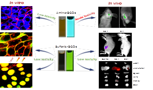
Both subcutaneous and orthotopic mice tumor models revealed thatthe sulfonic-GQDs showed specific targeting performance for the tumor tissues in vivo. Confocal images of frozen tumor and normal tissue sections further demonstrated the exceptional in vivo cancer-cell-nuclear-targeting capability of the sulfonic-GQDs, which showed no cancer type specificity. Both materials showed good performance for both in vitro and in vivo imaging, however, the toxicity issues of the amino-GQDs may limit their in vivo applications. Negatively charged sulfonic-GQDs showed low toxicity both in vitro and in vivo, which indicates their good potential for clinical applications.
Jinlong Liu
National Natural Science Foundation of China, China
Title: Luminescence characteristics and related damage evolution of carbon ion implanted GaN
Time : 17:05 - 17:20

Biography:
Jinlong Liu has his expertise in preparation and functional application of carbon materials including diamond, graphene, carbon dots and so on. He focuses on the mechanism of research on the carbon materials functional properties. He has researched the conductivity mechanism of H-terminated diamond and developed the MESFET devices. He also conducted research on luminescence mechanism of carbon dots prepared by micro wave heating and clarified the chemical reaction mechanism. In this work, he studied the defective evolution of carbon ion implanted GaN after annealing by slow positron annihilation, and the results will provide a framework to understand the behavior of carbon in GaN. It will be of great importance in expanding further application of C doped GaN.
Abstract:
Statement of the Problem: Carbon doped GaN has been widely studied and applied for p-type GaN and yellow light-emitting diodes. However, the sites carbon located, related with luminescence, characteristics has not been confirmed.
Methodology & Theoretical Orientation: GaN was implanted with carbon ion using dose of 1×1017 cm-2 and 2×1017 cm-2 and energy of 30 keV and 40 keV. And then the implanted samples were annealed at 800℃ for 20 min and 1 h under the N2 atmosphere. The luminescence characteristics of carbon ion implanted GaN was evaluated by PL spectrum with wavelength of 325 nm. The lattice damage of GaN was characterized by Raman spectrum and corresponding vacancy-defect evolution before and after annealing was measured by slow positron annihilation.

Conclusion & Significance: Most of carbon atoms would be located at the interstitial sites after carbon ion implantation due to the absorption of vacancies, and no obvious luminescence could be observed. As the implanted samples were annealed, strong yellow luminescence was emitted and the vacancy for N (VN) or vacancy for Ga (VGa) was reduced resulting from the migration of interstitial carbon (Ci) and formation of complex between them. By contrast, samples with higher dose showed stronger yellow light emission, which was related with the lower migration rate of Ci and saturated concentration of Ci-V complex.
Hussein Alrobei
University of South Florida, USA
Title: Aluminum -hematite nanocomposite films for photo electrochemical applications
Time : 17:20 - 17:35

Biography:
Hussein Alrobei is a PhD student under the supervision of Manoj K Ram. He has background in the field of Photo Electrochemical, Advanced Materials, Polymers and Energy. He has been involved on photo electrochemical properties on various metal oxides, polymers and conducting polymers, and recently his patent on nano-hybrid structured regioregular polyhexylthiophene blend films for production of photo electrochemical energy has been approved.
Abstract:
The alpha ( )–hematite (Fe2O3) based photoelectrochemical (PEC) devices are attractive due to splitting of water into hydrogen and oxygen, and it is has been studied extensively due to its bandgap, cost effectiveness, chemical stability and availability in nature. However, – Fe2O3 shows low carrier diffusion, higher resistivity, low electron mobility and higher photocorrosion. The mobility and carrier diffusion properties of –Fe2O3 can be improved by transition metal ion doping or making composite with metal oxide. So, attempt is made to make –Fe2O3 composite with aluminum (Al). Various ratios of Al with - Fe2O3 composite nanomaterials were synthesized using a sol-gel method. The Al- -Fe2O3 nanomaterial was characterized using SEM, FTIR and UV-vis techniques and X-ray diffraction, techniques. The cyclic voltammetric study was performed in three electrode cell where Al- - Fe2O3 worked as working electrode coated on conducting FTO glass plate, steel as counter and Ag/AgCl as reference electrode to estimate the diffusion coefficient and understanding of electrode/electrolyte interface. The Al doping has shown changes in the structural, optical, morphological and electrochemical properties of Al- -Fe2O3 compared to pristine - Fe2O3 photocatalyst. The photoelectrochemical properties of Al- - Fe2O3 based electrode has been understood through band diagrams. The photocurrent and band gap has clearly shown the improved hydrogen generation using Al- -Fe2O3 photocatalyst.
Dandan Xu
Beijing Forestry University, China
Title: Ionic liquid-stabilized graphene and its use in decorated with Co nano catalyst towards chlorinated organic pollutants degradation
Time : 17:35 - 17:50

Biography:
Dandan Xu is a Doctoral Candidate of Ecological Environment Engineering at Beijing Forestry University. She has been committed to environmental profession for 9 years. She has her expertise in electrochemical process to treat organic pollutants from the graduate studies. Her work on preparing electrocatalytic cathode based on ionic liquid creates new aspect for improving electrocatalytic performance. She has participated in several international conferences in many cities.
Abstract:
Tremendous efforts have been devoted to find methods with high-efficient and low-cost to remove chlorinated organic pollutant from aqueous solutions. Metal nanoparticles modified graphene materials have attracted considerable attention, but the limitation is the difficulty in depositing metal nanoparticles with uniform size and good dispersion on graphene surface. Ionic liquid (IL) shows potential for overcoming some of the above mentioned issues due to their high chemical and thermal stability, negligible vapor pressure, high conductivity and wide electrochemical window. This paper involved functionalization of graphene samples with IL ([Bmin][BF4]) and in situ reduction of cobalt precursors to improved their electrocatalytic performance and application on electrochemical degradation of chlorinated organic pollutants. Several characterization methods such as XRD, SEM and XPS were used to analyze prepared samples crystal structures, surface morphology, composition and nanoparticles size. XPS measurement showed the wide survey XPS pattern of catalyst, which indicated the coexistence of C, N, O and Co in the catalyst, and element N was originated from the IL. The sizes of Co nanoparticles on Co/IL-graphene (3.33 nm) was smaller than that on Co/graphene (6.60 nm) due to stabilization of IL.
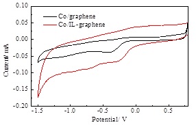
Electrocatalytic measurements revealed Co/IL-graphene catalysts displayed enhanced current response compared with Co/graphene samples. And a strong reduction peak at 0.036 V presented for Co/IL-graphene which was quite different from the Co/graphene catalyst. It indicated that the Co nanoparticles IL functionalized graphene had a significant electrocatalytic activity. The addition of IL can not only improve the dispersity of Co nanoparticle, but also increase the active sites. The Co/IL-graphene nanocomposite will be suitable materials for degradation of chlorinated organic pollutants in aqueous solutions.
- Graphene and other 2D materials
Location: .
Session Introduction
Steven Koester
University of Minnesota, USA
Title: Sensor Applications of Graphene Quantum Capacitance Varactors

Biography:
Dr. Koester received his Ph.D. in 1995 from the University of California, Santa Barbara. From 1997 to 2010 he was a research staff member at the IBM T. J. Watson Research Center and performed research on a wide variety of electronic and optoelectronic devices, with an emphasis on group-IV electronics. Since 2010, he has been a Professor of Electrical & Computer Engineering at the University of Minnesota where his research focuses on novel electronic, photonic and sensing device concepts with an emphasis on graphene and other 2D materials. Dr. Koester has authored or co-authored over 200 technical publications and conference presentations, 7 volumes, 4 book chapters, and holds 66 United States patents. He is an associate editor for IEEE Electron Device Letters and an IEEE Fellow.
Abstract:
Graphene has tremendous potential to form the basis of a powerful platform for biosensing due to its unique combination of properties, including high surface sensitivity, chemical stability, mechanical strength, and biocompatibility. However, to date, nearly all sensor concepts based upon graphene involve direct measurement of the electrical current in graphene. The need for direct electrical connections can limit the range of applications suitable for these devices, including many biological sensing functions, where wire leads can be cumbersome or impractical. In this talk, I will describe a novel sensor concept that utilizes a unique property of graphene, the quantum capacitance effect. The quantum capacitance effect in graphene allows the formation of a variable capacitor (or varactor) which, when integrated with an inductor, can form a passive LC resonator that can be interrogated through near-field inductive coupling. When the varactor is exposed to an external analyte (chemical, biological, etc.), the surface interaction of the analyte with the graphene shifts the charge concentration in the graphene, thus changing the capacitance and the resonant frequency of oscillation. With appropriate functionalization, this interaction can occur selectively to capture a specific chemical or biological target. We have developed a stable, high-yield fabrication process for graphene varactors utilizing a graphene grown by chemical vapor deposition and demonstrated devices with capacitance tuning ratios as high as 1.6-to-1. The varactor performance can be modeled very accurately utilizing a simple analytical model that takes into account disorder and charge trapping effects. We have demonstrated the operation of these devices for a variety of sensing applications, particularly for detection of glucose and acetone, important analytes for the treatment of diabetes. Finally, we have extensively analyzed the parasitic effect of water on the sensor performance and this work provides important insight into how the sensor robustness can be further improved.
Mineo Hiramatsu
Meijo University, Japan
Title: Carbon nanowalls, vertical nanographene network as platform for electrochemical application

Biography:
Prof. Mineo Hiramatsu is a Full Professor of Department of Electrical and Electronic Engineering and the Director of Nanocarbon Research Center, Meijo University, Japan. He also serves as the Director of Research Institute, Meijo University. He served as the Director of The Japan Society of Applied Physics. His main fields of research are plasma diagnostics and plasma processing for the synthesis of thin films and nanostructured materials. Author of more than 100 scientific papers and patents on plasma processes for materials science. Member of organizing and scientific committees of international conferences on plasma chemistry and plasma processing: International Conference on Reactive Plasmas, International Symposium on Advanced Plasma Science and its Applications for Nitrides and Nanomaterials, International Symposium on Dry Process, International Conference on Advanced Nanomaterials, THERMEC, International Conference on Processing & Manufacturing of Advanced Materials.
Abstract:
Carbon nanowalls (CNWs) are few-layer graphenes with open boundaries, standing vertically on a substrate. The sheets form a self-supported network of wall structures with thicknesses ranging from a few nanometers to a few tens of nanometers, and with a high aspect ratio. The maze-like architecture of CNWs with large-surface-area graphene planes would be useful as electrodes for energy storage devices, electrochemical and biosensors, and scaffold for cell culturing. From a practical point of view, structures of CNWs including spacing between adjacent nanowalls, crystallinity and alignment should be controlled according to the usage of CNWs. Moreover, post processes such as integration techniques including etching and coating of CNWs and surface functionalization should also be established. We report the current status of the control of the CNW structures during the growth processes as well as post treatment, together with examples of electrochemical applications using CNWs.
As an example of application, CNWs were used as platform for hydrogen peroxide (H2O2) sensing. This kind of application is based on the large surface area of conducting carbon and surface modifications including decoration with metal nanoparticles (NPs). It is known that H2O2 is a major messenger molecule in various redox-dependent cellular signaling transductions. Therefore, sensitive detection of H2O2 is greatly important in health inspection and environmental protections. For the H2O2 sensing, CNWs were grown on carbon fiber paper (CFP) using plasma-enhanced chemical vapor deposition with CH4/Ar mixture to increase the surface area. Then, CNW surface was decorated with Pt-NPs by the reduction of H2PtCl6 in solution. Cyclic voltammetry results showed that the Pt-decorated CNW/CFP electrode exhibited excellent electrocatalytic activity to the reduction of H2O2. Electrochemical experiments demonstrate that nanoplatform based on vertical nanographene offers great promise for providing a new class of nanostructured electrodes for electrochemical sensing, biosensing and energy conversion applications.
Kartik Ghosh
Missouri State University, USA
Title: Electrical and Magneto Transport Properties of Reduced Graphene Oxide Thin Films

Biography:
Ghosh has completed his PhD from Tata Institute of Fundamental Research and postdoctoral studies from the University of Maryland at College Park and Argonne National Laboratory. Currently, he is a Professor of Physics and Materials Science at Missouri State University. Over the last 25 years in his research career, he has been developing organic and inorganic thin films, nanomaterials, and their heterostructures for potential applications in the field of spintronics, renewable energy, and nanobiotechnology and has made important contributions to these fields. He has published over 150 peer-reviewed articles in highly cited journals and has been serving as a reviewer in many reputed journals.
Abstract:
Our goal is to follow a completely novel route to fabricate large area reduced graphene oxide (RGO) thin film using physical vapor deposition technique to achieve high charge carrier mobility with better conductivity. In order to avoid the chemical reagent based reduction path which often uses toxic reducing compound such as N2H4 and NaBH4, we used the pulsed laser deposition (PLD) technique. Large area uniform thin films of RGO were synthesized by PLD. A number of structural properties including the defect density, average size of sp2 clusters and degree of reduction have been investigated by Raman spectroscopy, X-ray photoelectron spectroscopy and x-ray diffraction. Temperature dependent (5K - 350K) four terminal electrical transport property measurement confirms variable range hopping and thermally activated transport mechanism of the charge carriers at low (5K - 210K) and high temperature (210K - 350K) regions, respectively. The calculated localization length, DOS near Fermi level (EF), hopping energy, and Arrhenius energy gap provide significant information to explain excellent electrical properties in the RGO films. Hall mobility measurement confirms p-type characteristics of the thin films. The charge carrier Hall mobility can be engineered by tuning the growth parameters, and the measured maximum mobility was 1596 cm2v-1s-1. The optimization of the improved electrical property is well supported by Raman spectroscopy. The transport properties of RGO samples are dependent on a number of factors including the density of the defect states, size of the sp2 clusters, degree of reduction, and the morphology of the thin film.

Biography:
Abstract:
- Nano Carbon Materials
Location: .
Session Introduction
Adam Khan
Akhan Semi conductors, USA
Title: Thin Film Nanocrystalline Diamond for Optical & Monolithically Integrated Display Applications

Biography:
Adam Khan is Founder & CEO of AKHAN Semiconductor and is currently leading the technology development program. Adam’s research interests include theoretical work in unconventional superconductor systems and applied work in n-type diamond semiconductor systems. Adam is listed inventor to over 11 issued and pending patents and has authored several published technical works in addition to roles co-chairing technical conferences and symposia. He is also the winner of a 2013 R&D 100 award, 2013 CleanTech Open Midwest Innovation Summit winner, and 2014 Forbes 30 under 30 in Energy & Industry. Adam earned his B.S. in Electrical Engineering and Physics from the University of Illinois Chicago, before pursuing graduate research at Stanford University’s Stanford Nanofabrication Facility.
Abstract:
Diamond is well-known for its extreme hardness, high-optical transparency, high thermal conductivity, and great chemical stability. In spite of all these excellent properties, diamond has largely been absent in optical applications due to the difficulty in fabricating high quality diamond thin films at lower substrate temperatures cost efficiently. Pioneering work on low temperature, high quality diamond deposition methods by AKHAN Semiconductor Inc. has opened doors for the use of diamond in a wide variety of optical applications. Nanocrystalline Diamond (NCD) coatings with grain size of 10-100 nm can significantly enhance the breakage, scratch performance and hydrophobicity of glass displays and lenses. In this work, NCD thin films of 50-250 nm thickness were deposited on commercial BK7 glass and chemically hardened Aluminosilicate Glass (Gorilla Glass) substrates (Figure 1 (a & b)) using Hot Filament and Microwave Plasma Chemical Vapor Deposition (HFCVD and MWCVD) techniques under optimized substrate temperatures to avoid substrate deformation. Optical characterization work of the as deposited NCD films was preformed using ellipsometry, spectral reflectance and spectrophotometry over visible wavelengths. Mechanical characterization work was also performed to obtain hardness & Young’s Modulus data for the NCD films. Measured results demonstrate the viability of NCD as a protective coating for a broad range of optical applications. Additionally, low temperature, high quality diamond deposition allows Complementary Metal Oxide Semiconductor (CMOS) device integration on optical substrates opening new opportunities for the development of next-generation monolithically integrated transparent devices and electronics.
Gibert Daniel Nessim
Bar Ilan University, Israel
Title: Towards the growth of 3D forests of carbon nanotubes: selective height control using reservoirs and overlayers

Biography:
The laboratory of Dr. Gilbert Daniel Nessim at Bar Ilan University (Israel) focuses on the synthesis of nanostructures using state-of-the-art chemical vapor deposition equipment. The scientific focus is to better understand the complex growth mechanisms of these nanostructures, to possibly functionalize them to tune their properties, and to integrate them into innovative devices.
Dr. Nessim joined the faculty of chemistry at Bar Ilan University in 2010 as lecturer and was promoted senior lecturer with tenure in 2014.
He holds a Ph.D in Materials Science and Engineering from the Massachusetts Institute of Technology (MIT), an MBA from INSEAD (France), and Masters in Electrical Engineering from the Politecnico di Milano and from the Ecole Centrale Paris (ECP, within the Erasmus/TIME program). Prior to his Ph.D, Dr. Nessim spent a decade in the high-tech industry and consulting across Europe, USA, and Israel.
Abstract:
Despite the massive progress achieved in the growth of carbon nanotube (CNT) forests on substrate, besides lithographic patterning of the catalyst, little has been done to selectively (locally) control CNT height. Varying process parameters, gases, catalysts, or underlayer materials uniformly affects CNT height over the whole substrate surface.We will show here how we can locally control CNT height, from no CNTs to up to 4X the nominal CNT height from iron catalyst on alumina underlayer by patterning reservoirs or by using overlayers during annealing or growth.
We pioneered the concept of reservoir showing how an iron thin film reservoir placed below the alumina underlayer almost doubles CNT height and how a copper/silver thin film reservoir deactivates the iron catalyst placed above it. We will also show how different thin film reservoir materials can enhance CNT growth by a factor of 4X.
We also pioneered the concept of overlayer, where a copper stencil or bridge placed above the catalyst surface during pre-annealing or during CNT growth deactivates the catalyst. We showed how we could pattern regions with CNTs and without CNTs by simply annealing the sample with a patterned overlayer positioned above its surface. Using nickel overlayers, we obtained a similar result but with a completely different mechanism. We thus synthesized patterned CNT forests using a simple process, without the need for lithography.
We can now combine the overlayer technique with one of the above-mentioned reservoirs (no reservoir, Cu/Ag reservoir, or Fe reservoir) to further modulate CNT growth by offsetting some or all of the growth enhancements achieved using the reservoirs. This modulation of the CNT height is a significant improvement compared to the "CNTs (one height) / no CNTs" patterning that has been achieved using lithography of the catalyst, and moves us closer to building 3D architectures of CNTs.
- Applications of Nano-diamond in drug delivery
Location: Chicago
- Carbon materials in energy
Location: .
Session Introduction
Ruchi Gakhar
University of Wisconsin, USA
Title: Characterization of graphite components of FHR design

Biography:
Ruchi Gakhar is a Postdoctoral research associate at UW Madison in the Department of Nuclear Engineering and Engineering Physics. She received her PhD in materials Science from University of Nevada, Reno in Decemeber 2015. She also holds an undergraduate and master's degree in chemistry and an additional master's in nanotechnology. During her PhD, she worked on designing of new, affordable materials to harness solar energy for clean energy production. She has published 15 journal articles and a book chapter so far.Ruchi has received several awards for academic excellence, including 2016 Nevada Regents' Scholar Award. At UW Madison, she is involved in investigating materials aspects of advanced nuclear reactor design – Fluoride salt cooled high temperature reactor (FHR).
Abstract:
Two types of graphite used in the core design of Fluoride Salt Cooled High Temperature Reactor (FHR) are Graphite Matrix A3 and Nuclear Grade IG110. Matrix A3 forms the structural component for the fuel kernels, while IG110 forms the reflector blocks and some of the internal core components[1]. Graphite forms an integral component of this design because it contributes to the structural integrity of the reactor as well as the pores of the graphite are considered as the main trapping site for the tritium produced in the coolant salt [2], [3]. Matrix A3 graphite which forms fuel pebble contains fission product that are produced during nuclear operation. In addition, the salt coolant or the corrosion products might intrude through the surface into the pores of the graphite [4]–[6]. Considering these attributes, the microstructure characterization of two grades of graphite is important in developing knowledge of characteristics of graphite under FHR operating conditions. The microstructural differences between A-3 and IG-110 are attributed to the differences in the raw materials and the heat treatment temperature during manufacturing [7]. The present study focuses on the microstructure examinationof two types of graphite components using X-ray Diffraction, Raman Spectroscopy, BET analysis, Mercury porosimetry and Scanning Electron Microscopy techniques. The lattice parameters, crystallite size (parallel and perpendicular to the basal plane), anisotropy and degree of graphitization estimated based on X-ray diffraction patterns and Raman spectra for both IG-110 and Matrix A3 graphite, will be discussed. The similarities and differences in microstructural characteristics between the two grades of graphite as obtained using the XRD and Raman spectroscopy results will be presented and the factors causing such differences will be discussed
Bingqing Wei
University of Delaware, USA
Title: Stretchable Energy Storage Systems Enabled by Engineering Nanostructured Carbon

Biography:
Dr. Bingqing (B. Q) Wei is currently a Full Professor in the Department of Mechanical Engineering at the University of Delaware. He was an Assistant Professor in the Department of Electrical & Computer Engineering and Center for Computation & Technology at Louisiana State University from 2003 to 2007. He had worked as a research scientist at Rensselaer Polytechnic Institute, Department of Materials Science and Engineering and Rensselaer Nanotechnology Center from 2000 to 2003. Dr. Wei was a visiting scientist for Max-Planck Institut für Metallforschung, Stuttgart, Germany in 1998 and 1999. From 1992 to 2001, he was a faculty member at Tsinghua University in Beijing, where he received his Bachelor’s degree (1987), M.S (1989), and Ph.D. (1992) in Mechanical Engineering. He is a member of The Materials Research Society (MRS), The Electrochemical Society (ECS), The American Chemical Society (ACS), and The American Society of Mechanical Engineering (ASME)
Abstract:
- Applications of carbon nanotubes
Location: .
Session Introduction
Pinar Camurlu
Akdeniz University, Turkey
Title: Fabrication of Electroactive Nanofibers

Biography:
Dr. Camurlu received her B.Sc. (1999), M.Sc (2001) and Ph.D. (2006) degrees from Department of Chemistry at Middle East Technical University in Ankara, Turkey. Dr. Camurlu has been working in Department of Chemistry at Akdeniz University (Antalya, Turkey) since 2007. Her research is focused on the design and synthesis of functional conjugated polymers and their applications such as; electrochromic devices, light emitting diodes, biosensors. She has published more than 45 papers in SCI journals and took part as a co-author for three international scientific book chapters.
Abstract:
Electroactive nanofibers, which are highly promising for sensor applications, have been receiving great attention due to their high electrical conductivity, surface area and porosity. Electrospinning has become one of the leading approaches for preparation of polymer nanofibers, owing to its superior attributes such as being simple, fast and relatively cheap. Focus of this study is to develop electroactive nanofibers based on conducting polymers which contain carbon nanotube (CNT).
The electroactive nanofibers, which were constituted from polyacrylonitrile (PAN), CNT and PEDOT, were fabricated by combining electrospinning and chemical vapor polymerization methods. The nanofiber mats were prepared by electrospinning of a PAN and CNT mixture in DMF. Later, these mats were subjected chemical vapor polymerization of EDOT in the presence of FeCl3. The resultant electroactive nanofibers were characterized by SEM, FTIR, CV and four point probe conductivity studies. The collective results have shown that the prepared mats contain conducting, homogeneous, electroactive PEDOT coatings on the surface of the PAN/CNT nanofibers, which are expected to be promising candidates for the fabrication of amperometric biosensors.
Hasan Erdem Camurlu
Akdeniz University, Turkey
Title: Preparation and Mechanical Properties of Carbon Nanotube Reinforced Aluminum Matrix Composites

Biography:
H. Erdem Çamurlu has completed his PhD in 2006 from Middle East Technical University, Ankara, Turkey. Currently, he is an Associate Professor in the Mechanical Engineering Department of Akdeniz University, Antalya, Turkey. He has published more than 35 papers in reputed journals.
Abstract:
Carbon nanotube (CNT) reinforced aluminum (unalloyed) matrix composites were produced by hot pressing powder metallurgical technique. Composites containing 0.25 – 3 wt.% CNT were obtained. Mixing was performed both by conventional ball milling (CBM) and high energy ball milling (HEBM). In CBM, which was performed solely for mixing purposes, zirconia balls having 2 mm diameter were used and milling was conducted for 15 minutes. In HEBM, a Retsch PM100 unit with tungsten carbide balls of 5 mm diameter was utilized, where mixing and grinding was conducted for 90 minutes at 150 rpm under argon atmosphere.
Hot pressing of the composites was performed at 600 oC for 30 minutes. Densities of the obtained composites were over 97% of theoretical.
In the microstructure of the composites obtained by CBM, carbon nanotubes were in the form of agglomerates and clusters. Thus, it was seen that conventional mixing was not sufficient for a good dispersion of CNT in Al. Hardness values were about 32.5 HB10 and did not change with the addition of CNT. 3 point bending strength of unreinforced sample was 295 MPa. There was a slight decrease in the strength and strain with increasing CNT content.In the composites obtained by HEBM, CNTs were seen to be well dispersed in the microstructure of the composites. Hardness was seen to be higher, as a result of the application of HEBM instead of CBM. Hardness of unreinforced Al increased to 42.5 HB10. Hardness of the composite containing 3 wt.% CNT reached a hardness value of 81.5 HB10. 3 point bending strength values were about 320 MPa and were not affected by the addition of CNT. Strain values of the composites were lower, as compared to unreinforced sample. Authors are grateful to Akdeniz University Scientific Research Projects Coordination Unit for supporting this project (FAY-2015-304).
- Diamond and Carbon in biology
Location: Chicago
- Large Scale Graphene production and characterization | Graphene and other 2D materials | Carbon nanotubes and Graphene | Novel hybrid carbon materials
Location: Zurich

Chair
Piotr Kula
Lodz University of technology, Poland

Co-Chair
James C Sung
Applied Diamonds Inc., Taiwan
Session Introduction
Piotr Kula
Lodz University of Technology, Poland
Title: High strength metallurgical graphene (HSMG®): Prospects for application in functional laminates and sensors
Time : 11:30 - 11:50

Biography:
P Kula, PhD, DSc, is the President of Polish Materials Society, a Member of European Materials Science Society (FEMS) and American Society for Metals. He has been the Head of Materials Science and Engineering Institute at Lodz University of Technology since 1997. Since then, he has founded and developed a strong research team in the field of Surface Engineering and Nanotechnology, recognized as the Lodz School. His main scientific and research achievements are non steady state models of vacuum carburizing and vacuum nitriding, artificial intelligence based software that supports these processes on the industrial scale and recently the manufacturing technology of high strength metallurgical graphene (HSMG) as well as the concept of using HSMG to produce the graphene-based nanocomposite for reversible storage of hydrogen
Abstract:
Effective practical application of products made of graphene as the base material are contingent on the development of methods of manufacturing large-area graphene on an industrial scale, the structure and properties of which would be similar to theoretical ones. At the Lodz University of Technology, an original industrial method was developed of producing large-area sheets of graphene through its controlled growth from metallic liquid phase. Graphene produced this way is close to structural perfection, i.e. it is single-layered and quasimonocrystalline, which results in its very high cohesion confirmed in static and cyclic tests of tensile strength. The authors of the 2D material produced in this manner called it "High Strength Metallurgical Graphene"–HSMG®. Also disclosed were two alternative growth mechanisms of graphene from the liquid metallic phase, i.e. dendritic and cellular, which produce HSMG with different electrical properties–respectively conductive graphene (c-HSMG), and semiconductive graphene (sc-HSMG). The capabilities of HSMG® were indicated with respect to selective adsorption and chemisorption of gases-in particular hydrogen-from gas mixtures. With the described mechanical and physical properties, high strength metallurgical graphene is ideal for application as the reinforcing phase and at the same time functionally active phase in laminates. HSMG can be repeatedly transferred between different substrates; this offers prospects of supervised control over the distance between successive reinforcement layers in the polymer matrix. A separate area of potential application of HSMG® is sensing of gases and electromagnetic radiation. The success of graphene as an engineering material of the future depends on the creative creation of new generation devices, rather than on strenuous attempts we have seen so far to replace other components with graphene in pre-existing design solutions and technologies.
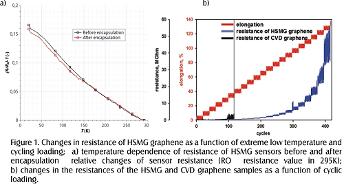
Steven Koester
University of Minnesota, USA
Title: Sensor Applications of Graphene Quantum Capacitance Varactors
Time : 11:50 - 12:10

Biography:
Steven J Koester has received his PhD in 1995 from the University of California, Santa Barbara. From 1997 to 2010, he was a Research Staff Member at the IBM T J Watson Research Center and performed research on a wide variety of electronic and optoelectronic devices, with an emphasis on group-IV electronics. Since 2010, he has been a Professor of Electrical and Computer Engineering at the University of Minnesota where his research focuses on novel electronic, photonic and sensing device concepts with an emphasis on graphene and other 2D materials. He has authored or co-authored over 200 technical publications and conference presentations, seven volumes, four book chapters, and holds 66 United States patents. He is an Associate Editor for IEEE Electron Device Letters and an IEEE Fellow.
Abstract:
Graphene has tremendous potential to form the basis of a powerful platform for bio sensing due to its unique combination of properties, including high surface sensitivity, chemical stability, mechanical strength, and biocompatibility. However, to date, nearly all sensor concepts based upon graphene involve direct measurement of the electrical current in graphene. The need for direct electrical connections can limit the range of applications suitable for these devices, including many biological sensing functions, where wire leads can be cumbersome or impractical. In this talk, I will describe a novel sensor concept that utilizes a unique property of graphene, the quantum capacitance effect. The quantum capacitance effect in graphene allows the formation of a variable capacitor (or varactor) which, when integrated with an inductor, can form a passive LC resonator that can be interrogated through near-field inductive coupling. When the varactor is exposed to an external analytes (chemical, biological, etc.), the surface interaction of the analytes with the graphene shifts the charge concentration in the graphene, thus changing the capacitance and the resonant frequency of oscillation. With appropriate functionalization, this interaction can occur selectively to capture a specific chemical or biological target. We have developed a stable, high-yield fabrication process for graphene varactor utilizing a graphene grown by chemical vapor deposition and demonstrated devices with capacitance tuning ratios as high as 1.6-to-1. The varactor performance can be modeled very accurately utilizing a simple analytical model that takes into account disorder and charge trapping effects. We have demonstrated the operation of these devices for a variety of sensing applications, particularly for detection of glucose and acetone, important analytes for the treatment of diabetes. Finally, we have extensively analyzed the parasitic effect of water on the sensor performance and this work provides important insight into how the sensor robustness can be further improved.
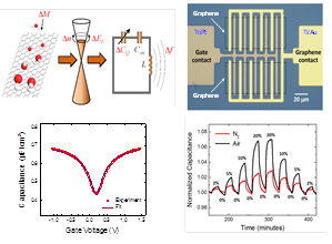
James C Sung
Applied Diamond Inc., Taiwan
Title: Large single crystal graphene production
Time : 12:10 - 12:30

Biography:
James C Sung was responsible for diamond production technology at GE Super Abrasives, for diamond tools development at Norton. He set the diamond grid specifications for diamond disks used worldwide for CMP of IC wafers, and helped IPO of Kink Company in Taiwan. He co-founded graphene synthetic with Huang-He worldwide, the world's largest diamond maker located in Henan China. He is now Chairman of Applied Diamond Inc., selling the most advanced CMP diamond disks-V the manufacture of next generation interconnects.
Abstract:
Graphene has phenomenal properties, such as 100X of steel’s tensile strength and 100X of copper’s electrical Conductivity. However, such properties depend on intact honeycomb structure of carbon atoms that may be present in natural graphite across nanometer scales of la or lc. In order to expand defects less graphite crystals to micron sizes. Honeycomb area about one million times, we invented a metal catalytic process to regrow graphite.
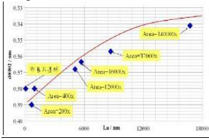
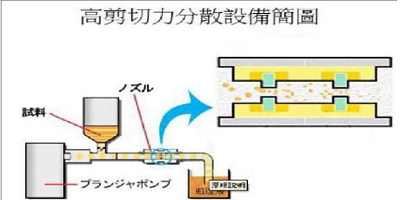 By heat treatment of nickel metal to saturate carbon atoms as solute, la can be enlarged with temperature and time as shown below. In addition to expand the single crystals of regrown graphite, we also exfoliate such single crystals by a liquid injection method with high pressure NMP that contains suspended graphite through a diamond nozzle. The supersonic speed of liquid can suddenly expand graphite to fewer layers. In the meantime, the defect ridden region of the regrown graphite is removed.
Mineo Hiramatsu
Meijo University, Japan
Title: Carbon nanowalls, vertical nanographene network as platform for electrochemical application
Time : 12:30 - 12:50

Biography:
Mineo Hiramatsu is a Full Professor of Department of Electrical and Electronic Engineering and the Director of Nanocarbon Research Center, Meijo University, Japan. He also serves as the Director of Research Institute, Meijo University. He served as the Director of The Japan Society of Applied Physics. His main fields of research are plasma diagnostics and plasma processing for the synthesis of thin films and nanostructured materials. He is the author of more than 100 scientific papers and patents on plasma processes for materials science. He is the Member of organizing and scientific committees of international conferences on plasma chemistry and plasma processing: International Conference on Reactive Plasmas, International Symposium on Advanced Plasma Science and its Applications for Nitrides and Nanomaterials, International Symposium on Dry Process, International Conference on Advanced Nanomaterials, THERMEC and International Conference on Processing and Manufacturing of Advanced Materials.
Abstract:
Carbon nanowalls (CNWs) are few-layer graphenes with open boundaries, standing vertically on a substrate. The sheets form a self-supported network of wall structures with thicknesses ranging from a few nanometers to a few tens of nanometers, and with a high aspect ratio. The maze-like architecture of CNWs with large-surface-area graphene planes would be useful as electrodes for energy storage devices, electrochemical and biosensors, and scaffold for cell culturing. From a practical point of view, structures of CNWs including spacing between adjacent nanowalls, crystallinity and alignment should be controlled according to the usage of CNWs. Moreover, post processes such as integration techniques including etching and coating of CNWs and surface functionalization should also be established. We report the current status of the control of the CNW structures during the growth processes as well as post treatment, together with examples of electrochemical applications using CNWs. As an example of application, CNWs were used as platform for hydrogen peroxide (H2O2) sensing. This kind of application is based on the large surface area of conducting carbon and surface modifications including decoration with metal nanoparticles (NPs). It is known that H2O2 is a major messenger molecule in various redox-dependent cellular signaling transductions. Therefore, sensitive detection of H2O2 is greatly important in health inspection and environmental protections.

For the H2O2 sensing, CNWs were grown on carbon fiber paper (CFP) using plasma-enhanced chemical vapor deposition with CH4/Ar mixture to increase the surface area. Then, CNW surface was decorated with Pt-NPs by the reduction of H2PtCl6 in solution. Cyclic voltammetry results showed that the Pt-decorated CNW/CFP electrode exhibited excellent electrocatalytic activity to the reduction of H2O2. Electrochemical experiments demonstrate that nano platform based on vertical nano graphene offers great promise for providing a new class of nanostructured electrodes for electrochemical sensing, biosensing and energy conversion applications.
Z Ryan Tian
Institute of Nanoscience / Engineering, USA
Title: Crosslinking graphene oxide flakes into nonflammable membrane for safe mass-production
Time : 12:50 - 13:10

Biography:
Z Ryan Tian directs nanosynthesis in both the Chemistry/Biochemistry Department, Institute of Nanoscience/Engineering, and R2R-printing in the High Density Electronics Center at UARK. He develops both new concepts/theories and industry-viable/scalable nanotechnologies e.g., ceramic nanofibers’ self-assemblies in nonwoven membrane for energy and medicine, new graphene materials, 3D-printable flexible concrete, etc. His inventions/patents were highlighted on AAAS-Eureka!, Science News, Science Daily, Discovery (News), NBC (TV Channel), Materials Today, ACS, ACerS, MRS, and shown to President Obama (in White House), President of India Dr. Abdul-Kalam (at UARK), Arkansas Governor, Arvest Bank-Owner Jim Walton, Wall Street nanotech-investor Scott Livingston, US iconic entrepreneur Larry Bock, et al. He has co-founded the J Nanotech. Engr. Med, Arkansas Institute of Nanoscience/Engineering, American Society of Nanomedicine, Global Nanomadicine Initiative, and served in numerous nanotech journals’ Editorial Boards. He got $45M grants into UARK, published 76 papers, 2 book-chapters, 5 patents (2 provisional), and 186 meeting/invited talks.
Abstract:
Graphene oxide (GO), a flake-like intermediate for making graphene from graphite, was proven by our lab and others’ to possess a fire hazard that can jeopardize the graphene large-scale production and wide applications. To solve this longstanding built-in problem, we have developed a simple, facile and scalable method for polymerizing the irregularly shaped/sized graphene oxide flakes with multivalent metal cations, such as Al3+, into a freestanding, mechanically strong, and paper-like flexible inflammable membrane in the form of a GO-oligomer. Thus-formed membrane that’s transparent to the naked eyes, about 10 um in thickness, resists in-air burning on an open flame (at which non-crosslinked graphene oxide was burnt out within ∼5 seconds), and resist hydrolysis in water over long time (during which non-crosslinked graphene oxide membrane quickly decomposes). Characterization data from SEM, HRTEM, XRD, microRaman, TGA/DSC, FTIR, and flame tests concluded that the multivalent cations effectively cross-linked the GO flakes, which in turn confirmed a strategy for polymerizing sheet-like nanomaterials in general.
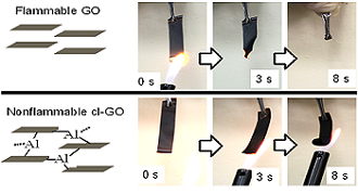
With the much improved on-flame and in-water stabilities, the membrane can enable e.g. roll-to-roll printing of high-temperature fuel cell membrane, battery membrane separators and electrodes, wearable electronics, flexible electronics, flexible thin-foil solar-cells, spray-able device packaging, sensors, etc. Other multivalent cations of transition metals and rare earth metals can likewise produce the new polymers with widely tunable electrical, magnetic and optical properties that ordinary graphene cannot possess.
Lunch Break: 13:15 - 13:55 @ Athens
Kartik Ghosh
Missouri State University, USA
Title: Electrical and Magneto Transport Properties of Reduced Graphene Oxide Thin Films
Time : 13:55 - 14:15

Biography:
Kartik Ghosh has completed his PhD from Tata Institute of Fundamental Research and Post-doctoral studies from the University of Maryland at College Park and Argonne National Laboratory. Currently, he is a Professor of Physics and Materials Science at Missouri State University. Over the last 25 years in his research career, he has been developing organic and inorganic thin films, nanomaterials, and their heterostructures for potential applications in the field of Spintronics, Renewable Energy, and Nano Biotechnology and has made important contributions to these fields. He has published over 150 peer-reviewed articles in highly cited journals and has been serving as a reviewer in many reputed journals.
Abstract:
Our goal is to follow a completely novel route to fabricate large area reduced graphene oxide (RGO) thin film using physical vapor deposition technique to achieve high charge carrier mobility with better conductivity. In order to avoid the chemical reagent based reduction path which often uses toxic reducing compound such as N2H4 and NaBH4, we used the pulsed laser deposition (PLD) technique. Large area uniform thin films of RGO were synthesized by PLD. A number of structural properties including the defect density, average size of sp2 clusters and degree of reduction have been investigated by Raman spectroscopy, X-ray photoelectron spectroscopy and x-ray diffraction. Temperature dependent (5K - 350K) four terminal electrical transport property measurements confirms variable range hopping and thermally activated transport mechanism of the charge carriers at low (5K - 210K) and high temperature (210K - 350K) regions, respectively. The calculated localization length, DOS near Fermi level (EF), hopping energy, and Arrhenius energy gap provide significant information to explain excellent electrical properties in the
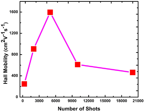
RGO films. Hall mobility measurement confirms p-type characteristics of the thin films. The charge carrier Hall mobility can be engineered by tuning the growth parameters, and the measured maximum mobility was 1596 cm2v-1s-1. The optimization of the improved electrical property is well supported by Raman spectroscopy. The transport properties of RGO samples are dependent on a number of factors including the density of the defect states, size of the sp2 clusters, degree of reduction, and the morphology of the thin film.
Gilbert Chahine
The National Centre for Scientific research, France
Title: Suspended graphene and nanoscrolls explored by nanofocused x-rays
Time : 14:15 - 14:35

Biography:
Gilbert Chahine is a Research-Engineer at the CNRS and working on the BM02 beamline at the European Synchrotron (ESRF) in Grenoble France. After a PhD in Materials Science with the highest distinction degree at the CEA in France, during his Post-doc he developed a new x-ray imaging technique (KMap) along with user-friendly software for the analysis of 5D data sets. This technique is now highly requested by a large community of researchers form international institutes to perform new types of experiments such as in situ and operando strain imaging, with the highest available resolution, of nano devices for photonics, photo voltaics and optoelectronics. Besides coordinating several projects involving international academic and industrial institutions in the field of strained semiconductors, he became interested in adapting the latest advances in synchrotron x-ray sources for a direct model-free in-depth probe of 2D materials’ local structure for a better understanding of their properties.
Abstract:
Structure determination of crystal lattice parameters and orientation with high precision is rather straightforward for bulk 3D-materials. X-ray diffraction proved especially powerful in this respect across the years. On the contrary, structural determination of 2D crystals with the help of x-rays is more demanding. So far, exploiting interferences between a crystalline substrate and graphene, it was possible to accurately determine the lattice parameter of graphene, averaged across the ~1cm2 surface of a sample. Such studies are however restricted to graphene samples of macroscopically uniform crystalline orientation. However most graphene samples of relevance for potential applications (micro-electronics, telecom, displays) exhibit in homogeneities, as they are composed of single-crystal grains (~10µm), each having different crystalline orientation and strain. Finely characterizing such structural features requires probing suspended graphene with the help of nano-shaped beams. Using, electron beams instead of nanofocused x-rays, we managed to conduct simultaneously small and wide angle x-ray scattering (SAXS/WAXS) characterizations with high resolution in reciprocal space and an unprecedented resolution of 200nm in real space, Accordingly we were able to map the structural variations in two- dimensions, revealing in this way strain maps for the suspended few-layer graphene membrane and the morphological features at the edges of the flakes, where it forms scrolls with a typical length of the order of 10µm and a diameter of the order of 10nm. The orientation of the nanoscrolls could for instance be resolved.
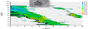
Our complementary analysis with spatially-resolved Raman spectroscopy provides the unique opportunity to unambiguously determine the Grüneisen parameters of graphene, linking the deformation to the energy of its vibration modes, without any particular assumption. These experiments pave the way to advance in-situ experiments and for exploring 2D crystals and their phase transitions using synchrotron radiation especially with the future upgrade programs in the European Synchrotron for outstanding expected brilliance.
Richard Clark
Morgan Advanced Materials, USA
Title: Graphene manufacture and simultaneous functionalization by electrochemical exfoliation – a winning paradigm or just another mark on an overpopulated IP map?
Time : 14:35 - 14:55

Biography:
Richard A Clark works at Morgan Advanced Materials (LSE: MGAM), is a UK-headquartered global manufacturer of specialized engineered products made from carbon, advanced ceramics and composites. After being educated as a Chemical Engineer, he has been with Morgan for 30 years, developing and commercializing materials across the spectrum of Morgan’s portfolio, most recently focusing on materials related to energy. He was part of Morgan’s team engaged with the University of Cambridge developing electrolytically produced carbon nanomaterials and has continued his involvement in this field in collaboration with Morgan’s team at the Manchester NGI.
Abstract:
Since the groundbreaking article in Science in October 2004 describing the occurrence, isolation and potential significance of graphene, there has been a huge interest in developing industrially scalable methods of manufacture from bottom-up and top-down routes. By mid-2015 the number of international patent applications had already exceeded 10,000 and the annual rate was continuing to accelerate exponentially. Over 11,000 scientific papers (more than one per hour) with graphene in the title were published in 2015. Hundreds of millions of dollars are being invested in such programs as Europe’s graphene flagship consortium as well in in many other academic and commercial organizations globally, although this far exceeds the current annual revenue of graphene producers, by an order of magnitude or more. One such top-down route developed for the mass manufacture of graphene involves electrochemical exfoliation. Promising in its own right, this can be performed using diazonium salts at a single applied potential, simultaneously functionalizing the single- or few-layer graphene generated. Not only does this remove the need for the secondary processing step, it is also a particularly effective means of separating the functionalized layers by virtue of the nitrogen generated during the in-situ diazonium reduction. Most typically for other top-down methods for production of graphene, functionalization is considered a separate, but necessary operation to permit dispersion, so this method appears to offer some clear economic advantages.
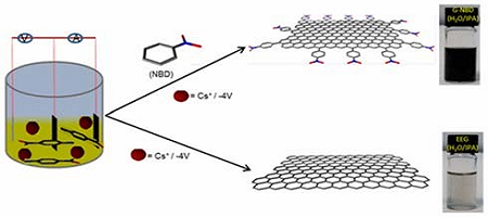
Although the method applies to a plurality of diazonium salts, nitrobenzenediazonium (NBD) salts are particularly effective as demonstrated by quantitative assessment of dispersibility and efficacy in improving capacitance at the laboratory scale. This presentation will review the current status of the graphene industry and specifically review the recent progress on electrochemical exfoliation in this context.
Guang Li
Donghua University, China
Title: The control of pore sizes in porous carbon fiber and its enhanced microwave absorption
Time : 14:55 - 15:15

Biography:
Guang Li has received her MSc degree in Chemistry from China Textile University in 1985 and PhD in Material Science and Engineering from Donghua University in 2006, respectively. She has worked as an Assistant Professor, a Lecturer and an Associate Professor at China Textile University from 1986 to 1999. She was a Senior Visiting Scholar in the University of Twente (Netherlands). She was promoted to be a full Professor at Donghua University (China) in 1999, and is continuously working on high performance polymer synthesis, porous carbon fibers and their associated processing for energy applications including PEM fuel cells. She has led more than 20 projects supported by Chinese National Natural Science Foundation, Ministry of Education of China, Shanghai Municipal Science and Technology Commission, etc. She has published more than 100 scientific papers in high-impacting peer-reviewed journals. She has given more than 24 keynote/invited/oral presentations in international conferences, co-authored 4 books and owns 26 patents. She has been awarded several prizes for recognizing her great contributions to science and technology, including the second prize of Science and Technology Progress in Shanghai, the second prize from Ministry of Education of China, the second prize from China Textile Industry Association, etc.
Abstract:
As one of the carbon materials, the porous carbon fiber has played a great role as catalyst support, separation by absorption; gas storage etc. based on its high aspect ratio. Among related publications, few studies focused on the microwave absorption characteristics of porous carbon fibers, although a great number of papers concerned carbon materials such as carbon black, fiber, tube as microwave absorbents. In this study, porous carbon fibers were prepared through carbonization of the blend fibers composed of poly (acrylonitrile) (PAN) and poly (methyl methacrylate) (PMMA) with 70 wt % of PAN. The pore size in porous carbon fibers could be controlled by changing the average molecular weight of PAN. The pores of 1-10μm and 0.1-1μm in diameter were obtained from the blend fibers where the average molecular weight of PAN is 51000 and 83000 g/mol, respectively (Figure 1). The obtained porous carbon fibers were used as absorbents to make epoxy composites with addition of 2-6 wt%. The microwave absorption properties were stimulated based on a model for a single-layer plane wave absorber. The results explained the porous carbon fiber showed much better microwave absorption than carbon nanofiber, and the porous carbon fiber with small size of pores showed much better microwave absorption than that with large size of pores, as shown in figure 2.
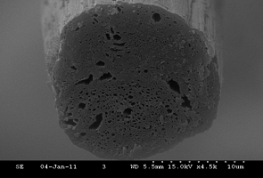
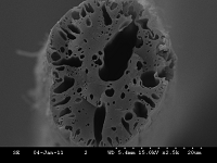
It is believed that the enhanced microwave absorption from the porous carbon fibers is due to a combination of the dielectric-type absorption and the interference of multi-reflected microwaves. When the pore size in porous carbon fibers is large, the air-absorber interfaces could be reduced at the same pore volume. Therefore, the superior microwave absorption of composites filled by porous carbon fiber with smaller pore size may be ascribed to the combination of absorption and interference of microwaves.
Steve Park
Korea Advanced Institute of Science and technology, South Korea
Title: The solution-based sorting and assembly of single-walled carbon nanotubes for transistors and pressure sensors
Time : 15:15 - 15:35

Biography:
Prof. Steve Park received his dual Bachelor’s degree in materials science and engineering and physics with magna cum laude from the University of Illinois at Urbana-Champaign and Knox College. He then worked as a technical staff for NanoInk Inc., developing commercial applications of dip-pen nanolithography. Prof. Park then received his Master of Science and Ph D from Stanford University in Materials Science and Engineering under the Prof. Zhenan Bao, researching on carbon nanotube and organic-based electronics. He then conducted his postdoctoral work at Columbia University in the electrical engineering and biomedical engineering department, working on piezoelectric polymer-based implantable devices
Abstract:
Single-walled carbon nanotubes (SWNTs) are an ideal channel material for next generation sub-10 nm gate-length transistors due to their ultra-thin body and high carrier transport properties. In addition, due to their high mechanical flexibility, SWNTs are an ideal candidate for flexible and stretchable sensors and electronics [1]. To use SWNTs as channel material in transistors, 1) semiconducting SWNTs must be fully separated from metallic SWNTs and 2) densely aligned over a large area, in a facile and scalable manner. To address the former, we have investigated solution-based sorting of SWNTs using various conjugated polymers.
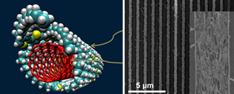
[2] With proper design of conjugated polymers, certain diameter range of the semiconducting SWNTs was selectively dispersed with high efficiency.[3] To address the latter, we have developed solution-shearing technique to densely align SWNTs over a large area, with density as high as 200 SWNTs/μm.[4] On-current density was improved by an order of magnitude over that of random network; however, with higher packing density, loss of electrostatic control was evident. These observations shed light on the behavior of aligned SWNT films and suggest possible approaches to further improve the electrical properties of SWNT-based transistors. We have also developed a stretchable capacitive tactile sensor based on carbon nanotube electrodes.[5] By buckling the carbon nanotubes into 'nanosprings,' high degree of stretchability up to 100% was attained. As the dielectric layer, we have implemented an air gap and a porous PDMS layer. The air gap enabled high sensitivity of 0.7 kPa^-1 in the low pressure regime (<1 kPa), while the porous PDMS layer enabled better pressure sensitivity in the tens of kPa regime. In addition, by simultaneously detecting the change in capacitance and the resistance of the top and bottom electrodes, various tactile inputs such as normal pressure, bending, and lateral strain was differentiated.
Coffee Break: 15:40 - 16:00 @ Foyer
- Graphene and other 2D materials
Location:
Session Introduction
Steven Koester
University of Minnesota, USA
Title: Sensor Applications of Graphene Quantum Capacitance Varactors

Biography:
Dr. Koester received his Ph.D. in 1995 from the University of California, Santa Barbara. From 1997 to 2010 he was a research staff member at the IBM T. J. Watson Research Center and performed research on a wide variety of electronic and optoelectronic devices, with an emphasis on group-IV electronics. Since 2010, he has been a Professor of Electrical & Computer Engineering at the University of Minnesota where his research focuses on novel electronic, photonic and sensing device concepts with an emphasis on graphene and other 2D materials. Dr. Koester has authored or co-authored over 200 technical publications and conference presentations, 7 volumes, 4 book chapters, and holds 66 United States patents. He is an associate editor for IEEE Electron Device Letters and an IEEE Fellow.
Abstract:
Graphene has tremendous potential to form the basis of a powerful platform for biosensing due to its unique combination of properties, including high surface sensitivity, chemical stability, mechanical strength, and biocompatibility. However, to date, nearly all sensor concepts based upon graphene involve direct measurement of the electrical current in graphene. The need for direct electrical connections can limit the range of applications suitable for these devices, including many biological sensing functions, where wire leads can be cumbersome or impractical. In this talk, I will describe a novel sensor concept that utilizes a unique property of graphene, the quantum capacitance effect. The quantum capacitance effect in graphene allows the formation of a variable capacitor (or varactor) which, when integrated with an inductor, can form a passive LC resonator that can be interrogated through near-field inductive coupling. When the varactor is exposed to an external analyte (chemical, biological, etc.), the surface interaction of the analyte with the graphene shifts the charge concentration in the graphene, thus changing the capacitance and the resonant frequency of oscillation. With appropriate functionalization, this interaction can occur selectively to capture a specific chemical or biological target. We have developed a stable, high-yield fabrication process for graphene varactors utilizing a graphene grown by chemical vapor deposition and demonstrated devices with capacitance tuning ratios as high as 1.6-to-1. The varactor performance can be modeled very accurately utilizing a simple analytical model that takes into account disorder and charge trapping effects. We have demonstrated the operation of these devices for a variety of sensing applications, particularly for detection of glucose and acetone, important analytes for the treatment of diabetes. Finally, we have extensively analyzed the parasitic effect of water on the sensor performance and this work provides important insight into how the sensor robustness can be further improved
Mineo Hiramatsu
Meijo University, Japan
Title: Carbon nanowalls, vertical nanographene network as platform for electrochemical application

Biography:
Prof. Mineo Hiramatsu is a Full Professor of Department of Electrical and Electronic Engineering and the Director of Nanocarbon Research Center, Meijo University, Japan. He also serves as the Director of Research Institute, Meijo University. He served as the Director of The Japan Society of Applied Physics. His main fields of research are plasma diagnostics and plasma processing for the synthesis of thin films and nanostructured materials. Author of more than 100 scientific papers and patents on plasma processes for materials science. Member of organizing and scientific committees of international conferences on plasma chemistry and plasma processing: International Conference on Reactive Plasmas, International Symposium on Advanced Plasma Science and its Applications for Nitrides and Nanomaterials, International Symposium on Dry Process, International Conference on Advanced Nanomaterials, THERMEC, International Conference on Processing & Manufacturing of Advanced Materials
Abstract:
Carbon nanowalls (CNWs) are few-layer graphenes with open boundaries, standing vertically on a substrate. The sheets form a self-supported network of wall structures with thicknesses ranging from a few nanometers to a few tens of nanometers, and with a high aspect ratio. The maze-like architecture of CNWs with large-surface-area graphene planes would be useful as electrodes for energy storage devices, electrochemical and biosensors, and scaffold for cell culturing. From a practical point of view, structures of CNWs including spacing between adjacent nanowalls, crystallinity and alignment should be controlled according to the usage of CNWs. Moreover, post processes such as integration techniques including etching and coating of CNWs and surface functionalization should also be established. We report the current status of the control of the CNW structures during the growth processes as well as post treatment, together with examples of electrochemical applications using CNWs.
As an example of application, CNWs were used as platform for hydrogen peroxide (H2O2) sensing. This kind of application is based on the large surface area of conducting carbon and surface modifications including decoration with metal nanoparticles (NPs). It is known that H2O2 is a major messenger molecule in various redox-dependent cellular signaling transductions. Therefore, sensitive detection of H2O2 is greatly important in health inspection and environmental protections. For the H2O2 sensing, CNWs were grown on carbon fiber paper (CFP) using plasma-enhanced chemical vapor deposition with CH4/Ar mixture to increase the surface area. Then, CNW surface was decorated with Pt-NPs by the reduction of H2PtCl6 in solution. Cyclic voltammetry results showed that the Pt-decorated CNW/CFP electrode exhibited excellent electrocatalytic activity to the reduction of H2O2. Electrochemical experiments demonstrate that nanoplatform based on vertical nanographene offers great promise for providing a new class of nanostructured electrodes for electrochemical sensing, biosensing and energy conversion applications.
Kartik Ghosh
Missouri State University, USA
Title: Electrical and Magneto Transport Properties of Reduced Graphene Oxide Thin Films

Biography:
Ghosh has completed his PhD from Tata Institute of Fundamental Research and postdoctoral studies from the University of Maryland at College Park and Argonne National Laboratory. Currently, he is a Professor of Physics and Materials Science at Missouri State University. Over the last 25 years in his research career, he has been developing organic and inorganic thin films, nanomaterials, and their heterostructures for potential applications in the field of spintronics, renewable energy, and nanobiotechnology and has made important contributions to these fields. He has published over 150 peer-reviewed articles in highly cited journals and has been serving as a reviewer in many reputed journals
Abstract:
Our goal is to follow a completely novel route to fabricate large area reduced graphene oxide (RGO) thin film using physical vapor deposition technique to achieve high charge carrier mobility with better conductivity. In order to avoid the chemical reagent based reduction path which often uses toxic reducing compound such as N2H4 and NaBH4, we used the pulsed laser deposition (PLD) technique. Large area uniform thin films of RGO were synthesized by PLD. A number of structural properties including the defect density, average size of sp2 clusters and degree of reduction have been investigated by Raman spectroscopy, X-ray photoelectron spectroscopy and x-ray diffraction. Temperature dependent (5K - 350K) four terminal electrical transport property measurement confirms variable range hopping and thermally activated transport mechanism of the charge carriers at low (5K - 210K) and high temperature (210K - 350K) regions, respectively. The calculated localization length, DOS near Fermi level (EF), hopping energy, and Arrhenius energy gap provide significant information to explain excellent electrical properties in the RGO films. Hall mobility measurement confirms p-type characteristics of the thin films. The charge carrier Hall mobility can be engineered by tuning the growth parameters, and the measured maximum mobility was 1596 cm2v-1s-1. The optimization of the improved electrical property is well supported by Raman spectroscopy. The transport properties of RGO samples are dependent on a number of factors including the density of the defect states, size of the sp2 clusters, degree of reduction, and the morphology of the thin film

Biography:
Morgan Advanced Materials (LSE: MGAM) is a UK-headquartered global manufacturer of specialized engineered products made from carbon, advanced ceramics and composites. It is one of two strategic partners for the graphene activities at the University of Manchester National Graphene Institute, Morgan being recognized by Manchester for having the product engineering and design expertise required to commercialize the materials developed at the NGI. After being educated as a chemical engineer, Richard Clark has been with Morgan for 30 years, developing and commercializing materials across the spectrum of Morgan’s portfolio, most recently focusing on materials related to energy. Richard was part of Morgan’s team engaged with the University of Cambridge developing electrolytically produced carbon nanomaterials and has continued his involvement in this field in collaboration with Morgan’s team at the Manchester NGI
Abstract:
Since the groundbreaking article in Science in October 2004 describing the occurrence, isolation and potential significance of graphene, there has been a huge interest in developing industrially scalable methods of manufacture from bottom-up and top-down routes. By mid-2015 the number of international patent applications had already exceeded 10,000 and the annual rate was continuing to accelerate exponentially. Over 11,000 scientific papers (more than one per hour) with “graphene” in the title were published in 2015. Hundreds of millions of dollars are being invested in such programs as Europe’s Graphene Flagship consortium as well in in many other academic and commercial organizations globally, although this far exceeds the current annual revenue of graphene producers, by an order of magnitude or more.One such top-down route developed for the mass manufacture of graphene involves electrochemical exfoliation. Promising in its own right, this can be performed using diazonium salts at a single applied potential, simultaneously functionalizing the single- or few-layer graphene generated. Not only does this remove the need for the secondary processing step, it is also a particularly effective means of separating the functionalized layers by virtue of the nitrogen generated during the in-situ diazonium reduction. Most typically for other top-down methods for production of graphene, functionalization is considered a separate, but necessary, operation to permit dispersion, so this method appears to offer some clear economic advantages. Although the method applies to a plurality of diazonium salts, nitrobenzenediazonium (NBD) salts are particularly effective as demonstrated by quantitative assessment of dispersibility and efficacy in improving capacitance at the laboratory scale. This presentation will review the current status of the graphene industry and specifically review the recent progress on electrochemical exfoliation in this context
Guang Li
Donghua University, China
Title: The control of pore sizes in porous carbon fiber and its enhanced microwave absorption

Biography:
Dr. Guang Li received her M.Sc in Chemistry from China Textile University in 1985, and her Ph.D in material science and engineering from Donghua University in 2006. She was a Senior Visiting Scholar in the University of Twente (Netherlands). She has been a full Professor at Donghua University sine 1999, and continuously working on high performance polymer , porous carbon fibers and their associated processing and applications. She has published more than 100 scientific papers in high-impacting peer-reviewed journals and has given more than 24 keynote/invited/oral presentations, co-authored 4 books, and owns 26 patents. Dr. Li has been awarded several prizes for recognizing her contributions to science and technology.
Abstract:
As one of carbon materials, the porous carbon fiber has played a great role as catalyst support, separation by absorption, gas storage etc. based its high aspect ratio. Among related publications, few studies focused on the microwave absorption characteristics of porous carbon fibers, although a great number of papers concerned carbon materials such as carbon black, fiber, tube as microwave absorbents[1-3]. In this study, Porous carbon fibers were prepared through carbonization of the blend fibers composed of poly(acrylonitrile) (PAN) and poly(methyl methacrylate) (PMMA)with 70 wt % of PAN. The pore size in porous carbon fibers could be controlled by changing the average molecular weight of PAN, The pores of 1-10μm and 0.1-1μm in diameter were obtained from the blend fibers where the average molecular weight of PAN is 51000 and 83000 g/mol, respectively(Figure 1). The obtained porous carbon fibers were used as absorbents to make epoxy composites with addition of 2-6 wt %. The microwave absorption properties were stimulated based on a model for a single-layer plane wave absorber. The results explained the porous carbon fiber showed much better microwave absorption than carbon nanofiber, and the porous carbon fiber with small size of pores showed much better microwave absorption than that with large size of pores, as shown in figure 2. It is believed that the enhanced microwave absorption from the porous carbon fibers is due to a combination of the dielectric-type absorption and the interference of multi-reflected microwaves[3-6]. When the pore size in porous carbon fibers is large, the air-absorber interfaces could be reduced at the same pore volume. Therefore, the superior microwave absorption of composites filled by porous carbon fiber with smaller pore size may be ascribed to the combination of absorption and interference of microwaves
- Graphene synthesis | Electrochemistry of diamond and nano carbon materials
Location: Zurich

Chair
Somnath Bhattacharya
University of Witwatersrand, South Africa

Co-Chair
Irina V Antonova
Institute of Semiconductor physics, Russia
Session Introduction
Irina V Antonova
Institute of Semiconductor Physics, Russia
Title: Graphene/fluorinated graphene systems for a wide spectrum of applications
Time : 16:00 - 16:20

Biography:
Irina V Antonova graduated from Department of Physics and Engineering, Novosibirsk State Technical University in 1979. Since 1981, she has been working in the Institute of Semiconductor Physics, Siberian Branch of the Russian Academy of Science. Presently, she occupies a leading Researcher Position at the Institute of Semiconductor Physics and heads a group of researchers who deal with investigation of graphene and its derivatives. Her activity was connected with transport and recharging phenomena in nanocomposite layers (Si, Ge nanocrystals in dielectric matrix), and localized states in heterostructures (SOI, quantum wells and quantum dots), high-pressure-related effects and surface passivation phenomena. The scope of her current research includes chemical functionalization of graphene, fabrication of graphene-based heterostructures and arrays of graphene quantum dots embedded in a fluorographene matrix, transport and recharging phenomena in nanocomposite layers. She has above 240 papers.
Abstract:
In the report we consider the properties of partially fluorinated graphene (FG) created with the use of a simple fluorination method based on the treatment in an aqueous solution of hydrofluoric acid. FG films can be formed from CVD grown graphene and a graphene suspension. A possibility to control a size of graphene flakes in a suspension in the course of their fluorination was also demonstrated. The possibility to create the FG films with arrays of graphene quantum dots (GQDs) is revealed. The spectrum of quantum confinement levels for GQDs in a fluorinated matrix and a charge relaxation time from GQDs are determined with the use of charge transient deep level spectroscopy. The time of GQD recharging can be controlled by means of GQD thickness variation or daylight assistance. This finding makes films with GQDs promising for flash memory applications. Fluorination of domain boundaries leads to a strong current modulation by gate voltage with an ON/OFF relation ~105 (the property important for field-effect transistors). The negative differential resistance (NDR) and a step-like increase in the current are found for films created from the fluorinated graphene suspension. The NDR resulting from the formation of a potential barrier system in the film is observed for a relatively low fluorination degree.
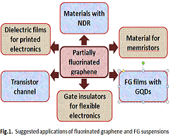
The observation of NDR in FG films widens the range of possible applications. A stable resistive switching effect is detected in films created from the FG suspension. The origin of resistive switching was found to connect with the appearance of traps with energy 0.08 eV and the recharging time lower than 700 ns. The charges in metal–insulator–semiconductor structures with FG dielectric layer have been estimated as the ultra-low values of (0.5–2) x1010 cm-2. Suspensions of fluorinated graphene with nanometer size flakes are of interest for the development of 2D ink-jet printing technologies and the production of thermally and chemically stable dielectric films for nanoelectronics on rigid and flexible substrates.
Omotayo A Arotiba
University of Johannesburg, South Africa
Title: The application of Diamond, Graphene and Exfoliated graphite in electrochemical sensing and electrochemical degradation of organic pollutants in water
Time : 16:20-16:40

Biography:
Omotayo A. Arotiba is an Electrochemist with expertise in the applications of nanomaterials such as carbons, dendrimers, metal/metal oxides for the development of (bio)sensors and photo-electrochemical systems for biomedical, environmental (water) related problems. He is currently involved in the development of electrochemical water treatment technologies as well as sensors for toxic metals, toxins and many substances of biomedical importance. He received his BSc (Hons) and MSc in Industrial Chemistry from the University of Ilorin and the University of Benin both in Nigeria. He obtained his PhD (in 2009) from the Department of Chemistry, University of the Western Cape, South Africa. He joined the Department of Applied Chemistry, University of Johannesburg in 2010 where he is currently a Professor. He is a member of the International Society of Electrochemistry, Royal Society of Chemistry and South African Chemical institute
Abstract:
This work presents an overview of our research on the use of carbon – diamond, graphene and exfoliated graphite – in the development of electrochemical sensors and photoanodic electrodes for the electrochemical degradation of organic water pollutants. In electrochemical sensing, a novel ternary composite electrode from diamond, graphene and polyaniline was prepared, characterised and applied for the electrochemical determination of 2,4-dichlorophenol (2,4-DCP) in aqueous media. The composite, obtained via the oxidative polymerisation of aniline in the presence of graphene and diamond, was characterised by FTIR spectroscopy, Raman spectroscopy etc and used to modify a glassy carbon electrode. The electrochemical properties of the bare and modified electrodes were investigated using cyclic voltammetry, square wave voltammetry (SWV) and impedance. The determination of 2,4-DCP in 0.1 M HNO3 was carried out using SWV and a detection limit of 0.25 μM was calculated.
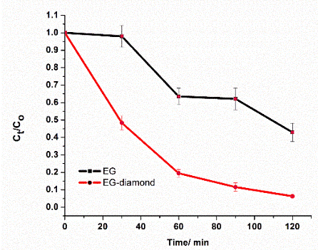
The electrode exhibited antifouling capabilities during the electro-oxidation of 2,4-DCP. For electrochemical degradation, composites electrode consisting of exfoliated graphite (EG) and diamond were prepared and used for the electrochemical degradation of organics in water. The extent of degradation of the organics was monitored with UV/VIS spectroscopy and total organic carbon. Results showed that the incorporation of diamond into EG yielded a more robust electrode in terms of current density and also enhanced the rate of degradation of the organics. This approach is promising for the development of alternative or complementary methods for water treatment
Karin Larrson
Uppsala University, Sweden
Title: Electronic Properties of Various B-doped Diamond(111)// Dye Molecule Interfaces
Time : 16:40 - 17:00

Biography:
Karin Larsson is a Professor in Inorganic Chemistry at the Department of Materials Chemistry, Uppsala University, Sweden. She is the leader of the Theoretical Materials Chemistry Group at the Department of Materials Chemistry. The scientific focus is on interpretation, understanding and prediction of the following processes/properties for both solid/gas interfaces, as well as for solid/liquid interfaces; i) CVD growth (incl. doping and its effect on surface properties), iii) interfacial processes for renewable energy applications (e.g. electrochemical processes), and iv) interfacial processes for e.g. bone regeneration (incl. biofunctionalisation of surfaces).
Abstract:
Diamond is a widely known material for its many excellent properties. A B-doped diamond is an excellent p-type material for solar cell usage. Due to some specific properties (e.g., large chemical inertness, very high carrier mobility for both electron and holes), it is considered as one of the strongest candidates for photovoltic electric generation. However, in order to implement the usage of diamond in solar energy applications, properties like the i) electrochemical window, ii) possibility for interfacial charge transfer, and iii) stability of functionalized surface, have to be further studied and optimized.
In the present investigation, the adsorption of different dye molecules onto H-terminated diamond (111) surfaces, have been theoretically studied using Density Functional Theory (DFT) calculations. The diamond surfaces were B-doped in order to make them p-type semi-conducting. The choice of dyes was based on the match between the electronic structures of these H-terminated B-doped diamond surfaces, and the respective dye molecules. The dye molecules in the present study included C20H13NO3S4 (A), C35H37NO2S3 (B), C34H38OS2(C), C32H36OS2(D), and C31H35S3Br(E). These dyes differ in the various functional groups, which have the role as electron acceptors. The main goal with the present study was thereby to investigate and compare the photovoltaic efficiency of the various dyes when attached to B-doped and H-terminated diamond (111) surfaces.
The calculated absortion spectra for in principle all of the different dyes were shown to be located in the most intense part of the sunlight spectrum.

Biography:
James C Sung was responsible for diamond production technology at GE Super Abrasives, for diamond tools development at Norton. He has set the diamond grid specifications for diamond disks used worldwide for CMP of IC wafers, and helped IPO of Kink Company in Taiwan. He co-founded graphene synthetic with Huang-He worldwide, the world's largest diamond maker located in Henan China. He is currently, the Chairman of Applied Diamond Inc., selling the most advanced CMP diamond disks-V the manufacture of next generation interconnects.
Abstract:
Graphene is the stretched diamond (111) plane graphene can be formed martensitic alloy without breaking the carbon bonds, on diamond surface by specialty heat treatment in vacuum. In this case graphene on diamond (GOD) hetero-epitaxy is similar to homo-epitaxy so the signal transmission is continuous. GOD is an ideal computational device as graphene contains the most effective transmission lattice, capable of terahertz communication by Mach 100 speed of phonon (lattice vibration). On the other hand, diamond is considered to be the most stable quantum computing solid due to its highest Debye temperature. During the quantum computing, the Q-bits must be entangled without atomic vibration, and diamond’s super hard lattice is capable to maintain this stability for milliseconds, even at room temperature. Diamond contains about 1% C13 isotope atoms in the lattice. These atoms may be ion planted and heat treated to cluster as Q-bits.
The superposition of spins from the extra neutron in the nuclei would be the best mechanism for quantum computing. With about 50 Q-bits entangled in milliseconds while these Q-bits are stationary, the vast computational possibilities can tackle even more difficult problems that for all human transistors combined. With GOD, the quantum computing can be initiated with graphene on cubical face (100) of diamond; and the collapsed quantum waves may exit from octahedral face (111). Thus, GOD would be the dream AI chip that outperforms even the smartest combinations of all current computers interconnected together.
Pralay Gayen
University of Illinois at Chicago, USA
Title: ¬¬¬Fluorination of Boron-doped Diamond Film Electrodes for Minimization of Perchlorate Formation
Time : 17:20 - 17:40

Biography:
Pralay Gayen has expertise in the area of electrochemical treatment of water and wastewater matrix. His research objective is to develop effective, highly robust and highly selective material to detect antibiotics, degrade different organics and inhibit perchlorate formation in water matrix as all these compounds pose serious health hazard. He has been using boron-doped diamond (BDD) electrodes for wastewater treatment as they are efficient at oxidizing recalcitrant organic compounds through electrochemical oxidation. He has also been using differently fluorinated BDD electrodes to prevent perchlorate formation without affecting organic oxidation as perchlorate is carcinogenic and formed through electrochemical oxidation of chloride. He also fabricated a sensor comprising BDD electrodes modified by carbon nanotube and nafion for the electrochemical detection of antibiotic (ciprofloxacin) in water and wastewater matrix as the presence of antibiotics for a long time will cause potential emergence of drug resistant bacteria.
Abstract:
The effects of surface fluorination on perchlorate formation rates as well as organic compound oxidation (phenol, terephthalic acid (TA)) rates at boron-doped diamond (BDD) film anodes were investigated. Different fluorination methods like electrochemical oxidation of perfluorooctanoic acid (PFOA) solutions, radio frequency plasma with H2/CF4 gas, and silanization with aliphatic (1H,1H,2H,2H perfluorodecyltrichlorosilane) and aromatic (triethoxy(pentafluorophenyl)silane) compounds have been used to incorporate fluorinated functional groups on the BDD surface, which was confirmed by X-ray photoelectron spectroscopy. The perchlorate formation rate was lowered by only 63.2% for PFOA modified BDD electrode and remained similar for both the plasma fluorinated and aromatic silanized BDD electrodes. However the perchlorate formation rate (<0.12 µmoles m-2 min-1) via chlorate and chloride oxidation was lowered by 99.96% and 99.95%, respectively, for aliphatic silanized electrode. The phenol oxidation rate decreased by 61% and 16.3% (with chloride) and TA oxidation decreased by 55% for the aliphatic silanized electrode. The apparent selectivity of the aliphatic silanized BDD electrode increased by 2.1-fold and 2.2-fold for TA and phenol, respectively whereas it decreased 680-fold for perchlorate formation. Fe(CN)63-/4- and Fe3+/2+ redox
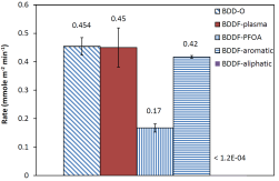
couples using cyclic voltammetry indicated that steric hindrance and hydrophobic effects between the fluorinated chains and chlorate ions may be responsible for the very low perchlorate formation on the aliphatic silanized (< 0.12 µmoles m-2 min-1) and PFOA modified electrodes (0.17 mmoles m-2 min-1). The PFOA modified BDD electrode showed a similar perchlorate formation rate after ageing, which confirmed high stability of the PFOA modification. The perchlorate formation rate was below the detection limit (<0.12 µmoles m-2 min-1) for up to 10 consecutive chlorate oxidation experiments and showed almost 90% decrease in perchlorate formation thereafter, which confirmed very high stability of aliphatic silanization under OHŸ production.
Marc Cretin
Université de Montpellier, France
Title: Carbon based materials: a promising approach for water depollution by electrochemical advanced oxidation processes
Time : 17:40 - 18:00

Biography:
Marc Cretin was born in France, in 1969. He received his Ph.D. degree in Electrochemistry (National Polytechnic
Institute of Grenoble France) in 1996 and joined Geneva University to develop electrochemical sensors for biomedical and environmental analysis. In 1998 he gained a position of assistant professor (ENSCM/Montpellier/France) to work on membranes materials for detection, separation and reaction. He’s full professor since 2012 at the University of Montpellier and works mainly in the field of materials for energ y and environment. He focuses his research mainly on electroactive materials for fuel cells, biofuel cells, EAOP (electrochemical advanced oxidation processes) and ceramic membranes for water treatment. He’s currently Director of the department “Physico-Chemistry, Interface and Polymer” at the European Membrane Institute of Montpellier (IEM) and co-director of the International French-Russia Laboratory MEIPA “Ion Exchange Membranes and Associated Processes”. Up to March 2017, he has co-authored more than 80 peer reviewed papers
Abstract:
Scarcity of pure water worldwide is dramatically affecting the economic development of Third Countries but also the industrial growth of others. Towards the water recycling and reuse, Electrochemical Advanced Oxidation Processes (EAOPs) are of high interest since they are very efficient in the degradation of refractory pollutants that cannot be eliminated by conventional techniques. Amongst them, the electro-Fenton (EF) process allows the in situ generation of highly reactive and nonselective hydroxyl radicals indirectly by cathodic oxygen reduction, its subsequent H2O2 production and further Fenton reaction (eq. 1).
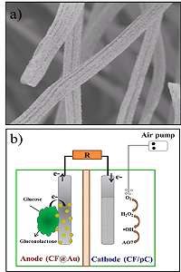
Fe2+ + H2O2 + H+ → Fe3+ + •OH + H2O (eq. 1)
Carbon felt is a good candidate to produce H2O2 from the reduction of dissolved oxygen [1] but it suffers from drawbacks like relatively low electronic conductivity and electrochemical active surface area. With the aim to increase carbon felt efficiency toward the electro-Fenton process, we develop in our research team, different modification routes to get microporous reactive carbon-based structures. It deals from basic thermal treatment under controlled atmosphere [2] to microporous carboneous coating prepared by combining Atomic Layer Deposition and solvothermal MOF growth on carbon felt [3], going through graphene functionalization [4] and LDH deposition for heterogeneous catalysis [5]. We will discuss synthesis, characterization and electrocatalytic properties of the different structures. Carbon based materials will be then integrated in a electrolysis system for water treatment but also in a prospective fuel cell – Fenton system for zero-energy water depollution [3]. Efficiency will be shown through the degradation and mineralization of pharmaceutical residues and organic dyes.
End of Day 1
