


Steve Park
Korea Advanced Institute of Science and technology, South Korea
Title: The solution-based sorting and assembly of single-walled carbon nanotubes for transistors and pressure sensors
Biography
Biography: Steve Park
Abstract
Single-walled carbon nanotubes (SWNTs) are an ideal channel material for next generation sub-10 nm gate-length transistors due to their ultra-thin body and high carrier transport properties. In addition, due to their high mechanical flexibility, SWNTs are an ideal candidate for flexible and stretchable sensors and electronics [1]. To use SWNTs as channel material in transistors, 1) semiconducting SWNTs must be fully separated from metallic SWNTs and 2) densely aligned over a large area, in a facile and scalable manner. To address the former, we have investigated solution-based sorting of SWNTs using various conjugated polymers.
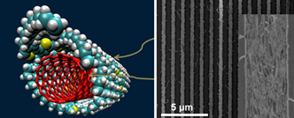
[2] With proper design of conjugated polymers, certain diameter range of the semiconducting SWNTs was selectively dispersed with high efficiency.[3] To address the latter, we have developed solution-shearing technique to densely align SWNTs over a large area, with density as high as 200 SWNTs/μm.[4] On-current density was improved by an order of magnitude over that of random network; however, with higher packing density, loss of electrostatic control was evident. These observations shed light on the behavior of aligned SWNT films and suggest possible approaches to further improve the electrical properties of SWNT-based transistors. We have also developed a stretchable capacitive tactile sensor based on carbon nanotube electrodes.[5] By buckling the carbon nanotubes into 'nanosprings,' high degree of stretchability up to 100% was attained. As the dielectric layer, we have implemented an air gap and a porous PDMS layer. The air gap enabled high sensitivity of 0.7 kPa^-1 in the low pressure regime (<1 kPa), while the porous PDMS layer enabled better pressure sensitivity in the tens of kPa regime. In addition, by simultaneously detecting the change in capacitance and the resistance of the top and bottom electrodes, various tactile inputs such as normal pressure, bending, and lateral strain was differentiated.