Day 1 :
Keynote Forum
Vijay K Arora
Wilkes University, USA
Keynote: Graphene nanoelectronics
Time : 09:00 - 09:25

Biography:
Vijay K Arora has obtained his PhD from the University of Colorado, USA. In addition to his tenured appointment at Wilkes University, he is privileged to have held the distinguished visiting appointments at the University of Tokyo, National University of Singapore, Nanyang Technological University, University of Western Australia and Universiti Teknologi Malaysia. He was Chair of NanoSingapore 2006, NanotechMalaysia 2010 and EscienceNano 2012 conferences. He is listed in a number of Who’s Who biographies. He has been invited to give keynote papers/lectures/courses at international forums, spanning from nanotechnology to nanoeducation to nanomanagement, both on and off a chip. He has published more than 100 papers in reputed journals and many uncounted publications in conference proceedings
Abstract:
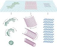
The rising era of graphene began with the award of the Nobel Prize in Physics 2010 jointly to Andre Geim and Konstantin Novoselov for groundbreaking experiments regarding the two-dimensional (2D) material with a honeybee lattice (Figure 1). Graphene can exist as 0D as fullerene, 1D as CNT, and 3D with multilayers. The experiments based on graphene have shown alternative material structures like phosphorene and silicene with expandable bandgap that is required for semiconductor devices. Its allotropes can form sensors as chemical elements react with the dangling bonds on the surface, thereby registering the presence of a chemical by enhanced transport properties. This review will first present the cohesive bandstructure as unique boundary conditions are applied to rolled-over graphene into CNT and small-width GNR, transforming 2D to 1D nanostructures. The transformed density of states and both the equilibrium and non-equilibrium distribution function define the carrier statistics and transformations of randomly oriented velocity vectors to streamlined ones in extreme non-equilibrium. Nonequilibrium Arora’s Distribution Function (NEADF) is shown to possess distinct properties that are considerably different from Monte Carlo procedures and Nonequilibrium Green’s function. The exceptional feature arising from the application of NEADF is the scattering-independence in the saturation region while ohmic mobility is strongly scattering-dependent. Moreover, it brings out vividly the velocity saturation as arising from the intrinsic velocity with a limiting value of the Graphene’s Fermi velocity that is higher than the Fermi velocity in semiconductors. Ballistic transport where device length is smaller than the scattering-limited mean free path is shown to degrade the mobility. Resistance quantum is obtained in 1D configuration that is generalized to give contact resistance and channel resistance. Magnetotransport in graphene is discussed to demonstrate the utilization of magnetic field in characterization and performance evaluation.
Keynote Forum
Orlando H Auciello
Professor of materials science and engineering and bioengineering, Distinguished Chair in Engineering
Keynote: Science and technology of multifunctional ultrananocrystalline diamond (UNCDTM) coatings and applications to a new generation of implantable medical devices
Time : 09:25 - 09:50

Biography:
Auciello graduated with M.S. (1973) and Ph.D (1976) degrees in Physics from the Physics Institute “Dr. Balseiro” (Universidad Nacional de Cuyo-Argentina). EE-University of Córdoba-Argentina (1970). Researcher-University of Toronto-Canada (1979-1984), Associate Professor-NCSU-USA (1985-1988), Distinguished Scientist-MCNC-USA (1988-1996), Distinguished Argonne Fellow (1996-2012)-Argonne National Laboratory-USA. Currently, Auciello is Distinguished Chair-University of Texas-Dallas. Auciello is directing basic/applied research programs on multifunctional oxide and novel ultrananocrystalline diamond (UNCD) thin films and application to industrial, high-tech, and medical devices. The UNCD film technology is commercialized for industrial products by Advanced Diamond Technologies, founded by Auciello and colleagues, (2003, profitable in 2014), and by Original Biomedical Implants (OBI-USA, 2013) and OBI-México (2016) for medical devices. Auciello edited 20 books and published about 500 articles in several fields, holds 20 patents, He is associate editor of APL and Integrated Ferroelectrics, He was President of the Materials Research Society (2013). Auciello is Fellow of AAAS and MRS
Abstract:
New paradigms in the research and development of nanocarbon thin films are providing the bases for new physics, new materials science and chemistry, and their impact in a new generation of multifunctional biomedical devices.
This talk will focus on discussing the science and technology of the new paradigm material named ultrananocrystalline diamond (UNCDTM) in thin film form and integration into a new generation of medical devices and implants as described below:
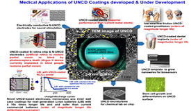
UNCD films co-developed and patented by O. Auciello and colleagues are synthesized by novel microwave plasma chemical vapor deposition and hot filament chemical vapor deposition techniques using an Ar-rich/CH4 chemistry that produces films with 2-5 nm grains. The fundamental science underlying the synthesis and properties of the UNCD films and applications to devices will be discussed. The UNCD films exhibit the lowest friction coefficient (0.02-0.04) compared with metals (≥ 0.5) currently used in many prostheses (e.g., hips, knees), electrically conductive UNCD coatings with nitrogen in grain boundaries can enable a new generation of neural electrodes, UNCD coatings are extremely biocompatible. Original Biomedical Implants (OBI-USA) and OBI-México, founded by Auciello and colleagues, are developing new generations of implantable medical devices based on the biocompatible UNCD coatings, namely: a) UNCD-coated silicon based microchip implantable inside the eye as a key component of the artificial retina to return partial vision blind by genetically-induced degeneration of photoreceptors; b) new generation of Li-ion batteries with ≥ 10x longer life and safer, using UNCD-based electrodes, membranes and inner wall battery case, enable next generation of defibrillator/pacemakers; c) new generation of implantable prostheses (e.g., dental implants, hips, knees) coated with UNCD eliminates failure of current metal-based implants due to synergistic mechanical wear / chemical corrosion by body fluids; d) UNCD-coated polymer with brain neurons tailored stiffness enables next generation less invasive electrodes for neural stimulation.
Keynote Forum
Kuan Tsae Huang
Aztrong Inc., USA
Keynote: Graphene battery: Impact on electrical vehicles and grid storage
Time : 09:50 - 10:15

Biography:
Kuan Tsae Huang is the CEO of AzTrong. He received his PhD in EECS from MIT and MS in Applied Math from Illinois-Urbana Champaign and BS from National Taiwan Normal University. He has extensive experience in commercializing technology in mass production, super capacitor and sensors/IoT for a wide range of industrial applications. He served as a Vice President of IBM and worked at IBM Watson Research Center and several start-ups, including SingaLab in Singapore, Nanotune in Mountain View and AzTrong in Taiwan. He was on the Faculty of number of universities in US, Singapore and Taiwan and President of National Taiwan Normal University. He was selected by LAUNCH as one of the 2011 top 10 Energy Innovators, which is organized by Department of State, NASA, USAID and NIKE. Currently, his focus is on graphene battery ranging from wearable/IoT devices to EV and Grid energy storage to Smart Life solution and services.
Abstract:
We expect that the graphene batteries will be the market leader for energy storage market in 2020. With the emergence of smart mobile devices (MD), electric vehicles (EV), and grid and distributed energy (G&DE), the world is moving rapidly towards a more connected and more sustainable place. Recent merge between Tesla and Solar City is an example. All these advances hinge upon the development of next generation of energy storage technologies that can deliver high energy and power densities at a low cost (i.e. $150/kWh) and high safety. Graphene has emerged as important candidate for electrode materials in lithium-ion batteries (LIBs) due to their unique physical properties. A review on the current state-of-the-art and most recent advances in graphene-containing nanocomposite electrodes and their derivatives will be provided along with the synthetic routes of their electrochemical performance in LIBs will be discussed. More importantly, the limitations of graphene related materials for energy storage applications will be highlighted, with an emphasis on anode and cathode materials. Several directions for near future R&D will be discussed. AzTrong is a leading production equipment supplier of high quality functional GO/rGO (ink, powder, slurry, film) for various applications & solutions. The author will share his experiences in graphene battery, graphene mass production as well as commercialization for energy storage and other applications.
Keynote Forum
Somnath Bhattacharya
University of Winwaterswand, Johannesburg
Keynote: Quantum device prospects of superconducting diamond films
Time : 10:15 - 10:40

Biography:
Somnath Bhattacharyya is a Professor in the School of Physics at the University of the Witwatersrand, Johannesburg, South Africa focusing on the area of condensed matter physics and nano-electronics. His major interest is in the transport properties of carbon and major achievements include the demonstration of resonant tunnel devices based on amorphous carbon, gigahertz transport in carbon devices, n-type doping of nanocrystalline diamond and developing theoretical models for transport in disordered carbon. His team focuses on the fabrication of the nanoelectronic devices, studying novel electronic properties of nanocrystalline diamond films and carbon superlattice structures at high magnetic fields and high frequencies. His group is also involved in performing theoretical modeling of carbon quantum structures. He is engaged in developing a new infrastructure for a wider range of nanotechnology that will include quantum matter, carbon based microwave detectors and nano-bio-electronics.
Abstract:
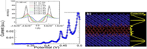
Nanostructured semiconducting carbon system, described by as a superlattice-like structure demonstrated its potential in switching device applications based on the quantum tunneling through the insulating carbon layer [1-4]. This switching property can be enhanced further with the association of Josephson’s tunneling between two superconducting carbon (diamond) grains separated by a very thin layer of carbon which holds the structure of the film firmly [5]. The superconducting nanodiamond heterostructures form qubits which can lead to the development of quantum computers provided the effect of disorder present in these structure can be firmly understood. Presently we concentrate on electrical transport properties of heavily boron–doped nanocrystalline diamond films around the superconducting transition temperature measured as a function of magnetic fields and the applied bias current. We demonstrate signature of anomalous negative Hall resistance in these films close to the superconductor-insulator-normal phase transition at low bias currents at zero magnetic field [5]. Current vs. voltage characteristics show signature of Josephson-like behavior which can give rise to a characteristic frequency of several hundred of gigahertz. Signature of spin flipping also shows novel spintronic device applications. We are working towards utilizing the superconducting phenomena in nanodiamond films in making some novel quantum electronic and high speed devices. This project complements our previous work on nitrogen-doped nanodiamond films and related nanostructured carbon devices which showed interesting radio frequency features in the gigahertz range.
Group Photo and Coffee Break: 10:40 -11:00 @ Foyer
Keynote Forum
Antonio Tejeda
Université Paris-Sud, France
Keynote: Gap opening and tailoring of graphene band structure
Time : 11:00 - 11:25

Biography:
Antonio Tejeda is a researcher at CNRS, the main French Research Center. He obtained a tenure position at CNRS in 2004, where he works at present in the Laboratoire de Physique des Solides. His areas of expertise are low dimensional systems, surfaces and interfaces, especially correlated surfaces and graphene. He often combines structural techniques and electronic spectroscopies, mainly scanning tunneling microscopy and high-resolution angle resolved photoemission.
Among his responsibilities are the chairing of the «International Symposium on Graphene Devices- 2012», the edition of a special issue on J. Phys. D: Appl. Phys on « Graphene: from functionalization to devices » and another on J. Phys.: Condens. Matter on « Correlation and many-body effects at surfaces ». He has also written the book “Photoemission in solids: concepts and applications”.
Abstract:
The disadvantage of graphene for using digital electronics is lack of bandgap, which is necessary to perform on-off switching operations in transistors. We have shown three different approaches to open a gap in graphene and tailor its electronic band structure. This includes (1) nanostructuration of graphene into graphene nanoribbons, (2) preparing a well-ordered buffer layer graphene and (3) introduction of a superperiodic potential in graphene grown on vicinal noble metal substrates.
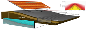
In our first approach to control graphene band structure, we have considered graphene ribbons grown on facets of the SiC(0001) surface. Our morphological characterization by scanning tunneling microscope (STM) and cross sectional transmission electron microscope (TEM) shows the presence mini-ribbons bordering a central extended ribbon. These mini-ribbons have a width of 1-2 nm and promote an electronic confinement gap of more than 0.5 eV as observed by photoemission, in an otherwise decoupled graphene from the substrate.
We have also studied the first stages of graphene growth. On SiC(0001) substrate, under adequate growth conditions, a well ordered first single layer graphene (i.e. the buffer layer) exhibits again a bandgap of more than 0.5eV. The origin of this bandgap was unclear, so we used STM, TEM angle-resolved photoemission spectroscopy (ARPES) together with calculations. This comprehensive study demonstrated that the bandgap opening is due to the super periodicity induced by the substrate.
Finally, we induced different superperiodicities on the underlying substrate to tailor graphene’s electronic properties. The nanostructuration of two substrates, Ir(332) and a multivicinal curved Pt(111) substrate induces a superperiodic potential on graphene that opens mini-gaps on the π band as observed by ARPES and consistent with the structural periodicity observed in STM and low energy electron diffraction.
- Diamond and Carbon in biology