Day 1 :
Keynote Forum
Vijay K Arora
Wilkes University, USA
Keynote: Graphene nanoelectronics
Time : 09:00 - 09:25

Biography:
Vijay K Arora has obtained his PhD from the University of Colorado, USA. In addition to his tenured appointment at Wilkes University, he is privileged to have held the distinguished visiting appointments at the University of Tokyo, National University of Singapore, Nanyang Technological University, University of Western Australia and Universiti Teknologi Malaysia. He was Chair of NanoSingapore 2006, NanotechMalaysia 2010 and EscienceNano 2012 conferences. He is listed in a number of Who’s Who biographies. He has been invited to give keynote papers/lectures/courses at international forums, spanning from nanotechnology to nanoeducation to nanomanagement, both on and off a chip. He has published more than 100 papers in reputed journals and many uncounted publications in conference proceedings
Abstract:
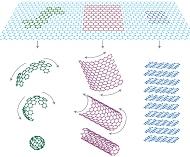
The rising era of graphene began with the award of the Nobel Prize in Physics 2010 jointly to Andre Geim and Konstantin Novoselov for groundbreaking experiments regarding the two-dimensional (2D) material with a honeybee lattice (Figure 1). Graphene can exist as 0D as fullerene, 1D as CNT, and 3D with multilayers. The experiments based on graphene have shown alternative material structures like phosphorene and silicene with expandable bandgap that is required for semiconductor devices. Its allotropes can form sensors as chemical elements react with the dangling bonds on the surface, thereby registering the presence of a chemical by enhanced transport properties. This review will first present the cohesive bandstructure as unique boundary conditions are applied to rolled-over graphene into CNT and small-width GNR, transforming 2D to 1D nanostructures. The transformed density of states and both the equilibrium and non-equilibrium distribution function define the carrier statistics and transformations of randomly oriented velocity vectors to streamlined ones in extreme non-equilibrium. Nonequilibrium Arora’s Distribution Function (NEADF) is shown to possess distinct properties that are considerably different from Monte Carlo procedures and Nonequilibrium Green’s function. The exceptional feature arising from the application of NEADF is the scattering-independence in the saturation region while ohmic mobility is strongly scattering-dependent. Moreover, it brings out vividly the velocity saturation as arising from the intrinsic velocity with a limiting value of the Graphene’s Fermi velocity that is higher than the Fermi velocity in semiconductors. Ballistic transport where device length is smaller than the scattering-limited mean free path is shown to degrade the mobility. Resistance quantum is obtained in 1D configuration that is generalized to give contact resistance and channel resistance. Magnetotransport in graphene is discussed to demonstrate the utilization of magnetic field in characterization and performance evaluation.
Keynote Forum
Orlando H Auciello
Professor of materials science and engineering and bioengineering, Distinguished Chair in Engineering
Keynote: Science and technology of multifunctional ultrananocrystalline diamond (UNCDTM) coatings and applications to a new generation of implantable medical devices
Time : 09:25 - 09:50

Biography:
Auciello graduated with M.S. (1973) and Ph.D (1976) degrees in Physics from the Physics Institute “Dr. Balseiro” (Universidad Nacional de Cuyo-Argentina). EE-University of Córdoba-Argentina (1970). Researcher-University of Toronto-Canada (1979-1984), Associate Professor-NCSU-USA (1985-1988), Distinguished Scientist-MCNC-USA (1988-1996), Distinguished Argonne Fellow (1996-2012)-Argonne National Laboratory-USA. Currently, Auciello is Distinguished Chair-University of Texas-Dallas. Auciello is directing basic/applied research programs on multifunctional oxide and novel ultrananocrystalline diamond (UNCD) thin films and application to industrial, high-tech, and medical devices. The UNCD film technology is commercialized for industrial products by Advanced Diamond Technologies, founded by Auciello and colleagues, (2003, profitable in 2014), and by Original Biomedical Implants (OBI-USA, 2013) and OBI-México (2016) for medical devices. Auciello edited 20 books and published about 500 articles in several fields, holds 20 patents, He is associate editor of APL and Integrated Ferroelectrics, He was President of the Materials Research Society (2013). Auciello is Fellow of AAAS and MRS
Abstract:
New paradigms in the research and development of nanocarbon thin films are providing the bases for new physics, new materials science and chemistry, and their impact in a new generation of multifunctional biomedical devices.
This talk will focus on discussing the science and technology of the new paradigm material named ultrananocrystalline diamond (UNCDTM) in thin film form and integration into a new generation of medical devices and implants as described below:
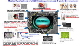
UNCD films co-developed and patented by O. Auciello and colleagues are synthesized by novel microwave plasma chemical vapor deposition and hot filament chemical vapor deposition techniques using an Ar-rich/CH4 chemistry that produces films with 2-5 nm grains. The fundamental science underlying the synthesis and properties of the UNCD films and applications to devices will be discussed. The UNCD films exhibit the lowest friction coefficient (0.02-0.04) compared with metals (≥ 0.5) currently used in many prostheses (e.g., hips, knees), electrically conductive UNCD coatings with nitrogen in grain boundaries can enable a new generation of neural electrodes, UNCD coatings are extremely biocompatible. Original Biomedical Implants (OBI-USA) and OBI-México, founded by Auciello and colleagues, are developing new generations of implantable medical devices based on the biocompatible UNCD coatings, namely: a) UNCD-coated silicon based microchip implantable inside the eye as a key component of the artificial retina to return partial vision blind by genetically-induced degeneration of photoreceptors; b) new generation of Li-ion batteries with ≥ 10x longer life and safer, using UNCD-based electrodes, membranes and inner wall battery case, enable next generation of defibrillator/pacemakers; c) new generation of implantable prostheses (e.g., dental implants, hips, knees) coated with UNCD eliminates failure of current metal-based implants due to synergistic mechanical wear / chemical corrosion by body fluids; d) UNCD-coated polymer with brain neurons tailored stiffness enables next generation less invasive electrodes for neural stimulation.
Keynote Forum
Kuan Tsae Huang
Aztrong Inc., USA
Keynote: Graphene battery: Impact on electrical vehicles and grid storage
Time : 09:50 - 10:15

Biography:
Kuan Tsae Huang is the CEO of AzTrong. He received his PhD in EECS from MIT and MS in Applied Math from Illinois-Urbana Champaign and BS from National Taiwan Normal University. He has extensive experience in commercializing technology in mass production, super capacitor and sensors/IoT for a wide range of industrial applications. He served as a Vice President of IBM and worked at IBM Watson Research Center and several start-ups, including SingaLab in Singapore, Nanotune in Mountain View and AzTrong in Taiwan. He was on the Faculty of number of universities in US, Singapore and Taiwan and President of National Taiwan Normal University. He was selected by LAUNCH as one of the 2011 top 10 Energy Innovators, which is organized by Department of State, NASA, USAID and NIKE. Currently, his focus is on graphene battery ranging from wearable/IoT devices to EV and Grid energy storage to Smart Life solution and services.
Abstract:
We expect that the graphene batteries will be the market leader for energy storage market in 2020. With the emergence of smart mobile devices (MD), electric vehicles (EV), and grid and distributed energy (G&DE), the world is moving rapidly towards a more connected and more sustainable place. Recent merge between Tesla and Solar City is an example. All these advances hinge upon the development of next generation of energy storage technologies that can deliver high energy and power densities at a low cost (i.e. $150/kWh) and high safety. Graphene has emerged as important candidate for electrode materials in lithium-ion batteries (LIBs) due to their unique physical properties. A review on the current state-of-the-art and most recent advances in graphene-containing nanocomposite electrodes and their derivatives will be provided along with the synthetic routes of their electrochemical performance in LIBs will be discussed. More importantly, the limitations of graphene related materials for energy storage applications will be highlighted, with an emphasis on anode and cathode materials. Several directions for near future R&D will be discussed. AzTrong is a leading production equipment supplier of high quality functional GO/rGO (ink, powder, slurry, film) for various applications & solutions. The author will share his experiences in graphene battery, graphene mass production as well as commercialization for energy storage and other applications.
Keynote Forum
Somnath Bhattacharya
University of Winwaterswand, Johannesburg
Keynote: Quantum device prospects of superconducting diamond films
Time : 10:15 - 10:40

Biography:
Somnath Bhattacharyya is a Professor in the School of Physics at the University of the Witwatersrand, Johannesburg, South Africa focusing on the area of condensed matter physics and nano-electronics. His major interest is in the transport properties of carbon and major achievements include the demonstration of resonant tunnel devices based on amorphous carbon, gigahertz transport in carbon devices, n-type doping of nanocrystalline diamond and developing theoretical models for transport in disordered carbon. His team focuses on the fabrication of the nanoelectronic devices, studying novel electronic properties of nanocrystalline diamond films and carbon superlattice structures at high magnetic fields and high frequencies. His group is also involved in performing theoretical modeling of carbon quantum structures. He is engaged in developing a new infrastructure for a wider range of nanotechnology that will include quantum matter, carbon based microwave detectors and nano-bio-electronics.
Abstract:
Nanostructured semiconducting carbon system, described by as a superlattice-like structure demonstrated its potential in switching device applications based on the quantum tunneling through the insulating carbon layer [1-4]. This switching property can be enhanced further with the association of Josephson’s tunneling between two superconducting carbon (diamond) grains separated by a very thin layer of carbon which holds the structure of the film firmly [5]. The superconducting nanodiamond heterostructures form qubits which can lead to the development of quantum computers provided the effect of disorder present in these structure can be firmly understood. Presently we concentrate on electrical transport properties of heavily boron–doped nanocrystalline diamond films around the superconducting transition temperature measured as a function of magnetic fields and the applied bias current. We demonstrate signature of anomalous negative Hall resistance in these films close to the superconductor-insulator-normal phase transition at low bias currents at zero magnetic field [5]. Current vs. voltage characteristics show signature of Josephson-like behavior which can give rise to a characteristic frequency of several hundred of gigahertz. Signature of spin flipping also shows novel spintronic device applications. We are working towards utilizing the superconducting phenomena in nanodiamond films in making some novel quantum electronic and high speed devices. This project complements our previous work on nitrogen-doped nanodiamond films and related nanostructured carbon devices which showed interesting radio frequency features in the gigahertz range.
Group Photo and Coffee Break: 10:40 -11:00 @ Foyer
Keynote Forum
Antonio Tejeda
Université Paris-Sud, France
Keynote: Gap opening and tailoring of graphene band structure
Time : 11:00 - 11:25

Biography:
Antonio Tejeda is a researcher at CNRS, the main French Research Center. He obtained a tenure position at CNRS in 2004, where he works at present in the Laboratoire de Physique des Solides. His areas of expertise are low dimensional systems, surfaces and interfaces, especially correlated surfaces and graphene. He often combines structural techniques and electronic spectroscopies, mainly scanning tunneling microscopy and high-resolution angle resolved photoemission.
Among his responsibilities are the chairing of the «International Symposium on Graphene Devices- 2012», the edition of a special issue on J. Phys. D: Appl. Phys on « Graphene: from functionalization to devices » and another on J. Phys.: Condens. Matter on « Correlation and many-body effects at surfaces ». He has also written the book “Photoemission in solids: concepts and applications”.
Abstract:
The disadvantage of graphene for using digital electronics is lack of bandgap, which is necessary to perform on-off switching operations in transistors. We have shown three different approaches to open a gap in graphene and tailor its electronic band structure. This includes (1) nanostructuration of graphene into graphene nanoribbons, (2) preparing a well-ordered buffer layer graphene and (3) introduction of a superperiodic potential in graphene grown on vicinal noble metal substrates.
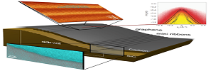
In our first approach to control graphene band structure, we have considered graphene ribbons grown on facets of the SiC(0001) surface. Our morphological characterization by scanning tunneling microscope (STM) and cross sectional transmission electron microscope (TEM) shows the presence mini-ribbons bordering a central extended ribbon. These mini-ribbons have a width of 1-2 nm and promote an electronic confinement gap of more than 0.5 eV as observed by photoemission, in an otherwise decoupled graphene from the substrate.
We have also studied the first stages of graphene growth. On SiC(0001) substrate, under adequate growth conditions, a well ordered first single layer graphene (i.e. the buffer layer) exhibits again a bandgap of more than 0.5eV. The origin of this bandgap was unclear, so we used STM, TEM angle-resolved photoemission spectroscopy (ARPES) together with calculations. This comprehensive study demonstrated that the bandgap opening is due to the super periodicity induced by the substrate.
Finally, we induced different superperiodicities on the underlying substrate to tailor graphene’s electronic properties. The nanostructuration of two substrates, Ir(332) and a multivicinal curved Pt(111) substrate induces a superperiodic potential on graphene that opens mini-gaps on the π band as observed by ARPES and consistent with the structural periodicity observed in STM and low energy electron diffraction.
- Large Scale Graphene production and characterization | Graphene and other 2D materials | Carbon nanotubes and Graphene | Novel hybrid carbon materials
Location: Zurich

Chair
Piotr Kula
Lodz University of technology, Poland

Co-Chair
James C Sung
Applied Diamonds Inc., Taiwan
Session Introduction
Piotr Kula
Lodz University of Technology, Poland
Title: High strength metallurgical graphene (HSMG®): Prospects for application in functional laminates and sensors
Time : 11:30 - 11:50

Biography:
P Kula, PhD, DSc, is the President of Polish Materials Society, a Member of European Materials Science Society (FEMS) and American Society for Metals. He has been the Head of Materials Science and Engineering Institute at Lodz University of Technology since 1997. Since then, he has founded and developed a strong research team in the field of Surface Engineering and Nanotechnology, recognized as the Lodz School. His main scientific and research achievements are non steady state models of vacuum carburizing and vacuum nitriding, artificial intelligence based software that supports these processes on the industrial scale and recently the manufacturing technology of high strength metallurgical graphene (HSMG) as well as the concept of using HSMG to produce the graphene-based nanocomposite for reversible storage of hydrogen
Abstract:
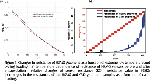
Effective practical application of products made of graphene as the base material are contingent on the development of methods of manufacturing large-area graphene on an industrial scale, the structure and properties of which would be similar to theoretical ones. At the Lodz University of Technology, an original industrial method was developed of producing large-area sheets of graphene through its controlled growth from metallic liquid phase. Graphene produced this way is close to structural perfection, i.e. it is single-layered and quasimonocrystalline, which results in its very high cohesion confirmed in static and cyclic tests of tensile strength. The authors of the 2D material produced in this manner called it "High Strength Metallurgical Graphene"–HSMG®. Also disclosed were two alternative growth mechanisms of graphene from the liquid metallic phase, i.e. dendritic and cellular, which produce HSMG with different electrical properties–respectively conductive graphene (c-HSMG), and semiconductive graphene (sc-HSMG). The capabilities of HSMG® were indicated with respect to selective adsorption and chemisorption of gases-in particular hydrogen-from gas mixtures. With the described mechanical and physical properties, high strength metallurgical graphene is ideal for application as the reinforcing phase and at the same time functionally active phase in laminates. HSMG can be repeatedly transferred between different substrates; this offers prospects of supervised control over the distance between successive reinforcement layers in the polymer matrix. A separate area of potential application of HSMG® is sensing of gases and electromagnetic radiation. The success of graphene as an engineering material of the future depends on the creative creation of new generation devices, rather than on strenuous attempts we have seen so far to replace other components with graphene in pre-existing design solutions and technologies.
Steven Koester
University of Minnesota, USA
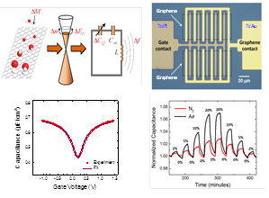
Title: Sensor Applications of Graphene Quantum Capacitance Varactors
Time : 11:50 - 12:10

Biography:
Steven J Koester has received his PhD in 1995 from the University of California, Santa Barbara. From 1997 to 2010, he was a Research Staff Member at the IBM T J Watson Research Center and performed research on a wide variety of electronic and optoelectronic devices, with an emphasis on group-IV electronics. Since 2010, he has been a Professor of Electrical and Computer Engineering at the University of Minnesota where his research focuses on novel electronic, photonic and sensing device concepts with an emphasis on graphene and other 2D materials. He has authored or co-authored over 200 technical publications and conference presentations, seven volumes, four book chapters, and holds 66 United States patents. He is an Associate Editor for IEEE Electron Device Letters and an IEEE Fellow.
Abstract:
Graphene has tremendous potential to form the basis of a powerful platform for bio sensing due to its unique combination of properties, including high surface sensitivity, chemical stability, mechanical strength, and biocompatibility. However, to date, nearly all sensor concepts based upon graphene involve direct measurement of the electrical current in graphene. The need for direct electrical connections can limit the range of applications suitable for these devices, including many biological sensing functions, where wire leads can be cumbersome or impractical. In this talk, I will describe a novel sensor concept that utilizes a unique property of graphene, the quantum capacitance effect. The quantum capacitance effect in graphene allows the formation of a variable capacitor (or varactor) which, when integrated with an inductor, can form a passive LC resonator that can be interrogated through near-field inductive coupling. When the varactor is exposed to an external analytes (chemical, biological, etc.), the surface interaction of the analytes with the graphene shifts the charge concentration in the graphene, thus changing the capacitance and the resonant frequency of oscillation. With appropriate functionalization, this interaction can occur selectively to capture a specific chemical or biological target. We have developed a stable, high-yield fabrication process for graphene varactor utilizing a graphene grown by chemical vapor deposition and demonstrated devices with capacitance tuning ratios as high as 1.6-to-1. The varactor performance can be modeled very accurately utilizing a simple analytical model that takes into account disorder and charge trapping effects. We have demonstrated the operation of these devices for a variety of sensing applications, particularly for detection of glucose and acetone, important analytes for the treatment of diabetes. Finally, we have extensively analyzed the parasitic effect of water on the sensor performance and this work provides important insight into how the sensor robustness can be further improved.
James C Sung
Applied Diamond Inc., Taiwan
Title: Large single crystal graphene production
Time : 12:10 - 12:30

Biography:
James C Sung was responsible for diamond production technology at GE Super Abrasives, for diamond tools development at Norton. He set the diamond grid specifications for diamond disks used worldwide for CMP of IC wafers, and helped IPO of Kink Company in Taiwan. He co-founded graphene synthetic with Huang-He worldwide, the world's largest diamond maker located in Henan China. He is now Chairman of Applied Diamond Inc., selling the most advanced CMP diamond disks-V the manufacture of next generation interconnects.
Abstract:
Graphene has phenomenal properties, such as 100X of steel’s tensile strength and 100X of copper’s electrical Conductivity. However, such properties depend on intact honeycomb structure of carbon atoms that may be present in natural graphite across nanometer scales of la or lc. In order to expand defects less graphite crystals to micron sizes. Honeycomb area about one million times, we invented a metal catalytic process to regrow graphite.
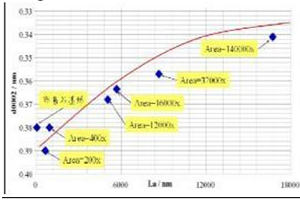
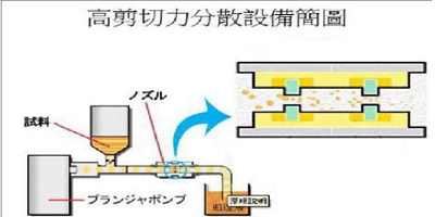 By heat treatment of nickel metal to saturate carbon atoms as solute, la can be enlarged with temperature and time as shown below. In addition to expand the single crystals of regrown graphite, we also exfoliate such single crystals by a liquid injection method with high pressure NMP that contains suspended graphite through a diamond nozzle. The supersonic speed of liquid can suddenly expand graphite to fewer layers. In the meantime, the defect ridden region of the regrown graphite is removed.
Mineo Hiramatsu
Meijo University, Japan
Title: Carbon nanowalls, vertical nanographene network as platform for electrochemical application
Time : 12:30 - 12:50

Biography:
Mineo Hiramatsu is a Full Professor of Department of Electrical and Electronic Engineering and the Director of Nanocarbon Research Center, Meijo University, Japan. He also serves as the Director of Research Institute, Meijo University. He served as the Director of The Japan Society of Applied Physics. His main fields of research are plasma diagnostics and plasma processing for the synthesis of thin films and nanostructured materials. He is the author of more than 100 scientific papers and patents on plasma processes for materials science. He is the Member of organizing and scientific committees of international conferences on plasma chemistry and plasma processing: International Conference on Reactive Plasmas, International Symposium on Advanced Plasma Science and its Applications for Nitrides and Nanomaterials, International Symposium on Dry Process, International Conference on Advanced Nanomaterials, THERMEC and International Conference on Processing and Manufacturing of Advanced Materials.
Abstract:
Carbon nanowalls (CNWs) are few-layer graphenes with open boundaries, standing vertically on a substrate. The sheets form a self-supported network of wall structures with thicknesses ranging from a few nanometers to a few tens of nanometers, and with a high aspect ratio. The maze-like architecture of CNWs with large-surface-area graphene planes would be useful as electrodes for energy storage devices, electrochemical and biosensors, and scaffold for cell culturing. From a practical point of view, structures of CNWs including spacing between adjacent nanowalls, crystallinity and alignment should be controlled according to the usage of CNWs. Moreover, post processes such as integration techniques including etching and coating of CNWs and surface functionalization should also be established. We report the current status of the control of the CNW structures during the growth processes as well as post treatment, together with examples of electrochemical applications using CNWs. As an example of application, CNWs were used as platform for hydrogen peroxide (H2O2) sensing. This kind of application is based on the large surface area of conducting carbon and surface modifications including decoration with metal nanoparticles (NPs). It is known that H2O2 is a major messenger molecule in various redox-dependent cellular signaling transductions. Therefore, sensitive detection of H2O2 is greatly important in health inspection and environmental protections.

For the H2O2 sensing, CNWs were grown on carbon fiber paper (CFP) using plasma-enhanced chemical vapor deposition with CH4/Ar mixture to increase the surface area. Then, CNW surface was decorated with Pt-NPs by the reduction of H2PtCl6 in solution. Cyclic voltammetry results showed that the Pt-decorated CNW/CFP electrode exhibited excellent electrocatalytic activity to the reduction of H2O2. Electrochemical experiments demonstrate that nano platform based on vertical nano graphene offers great promise for providing a new class of nanostructured electrodes for electrochemical sensing, biosensing and energy conversion applications.
Z Ryan Tian
Institute of Nanoscience / Engineering, USA
Title: Crosslinking graphene oxide flakes into nonflammable membrane for safe mass-production
Time : 12:50 - 13:10

Biography:
Z Ryan Tian directs nanosynthesis in both the Chemistry/Biochemistry Department, Institute of Nanoscience/Engineering, and R2R-printing in the High Density Electronics Center at UARK. He develops both new concepts/theories and industry-viable/scalable nanotechnologies e.g., ceramic nanofibers’ self-assemblies in nonwoven membrane for energy and medicine, new graphene materials, 3D-printable flexible concrete, etc. His inventions/patents were highlighted on AAAS-Eureka!, Science News, Science Daily, Discovery (News), NBC (TV Channel), Materials Today, ACS, ACerS, MRS, and shown to President Obama (in White House), President of India Dr. Abdul-Kalam (at UARK), Arkansas Governor, Arvest Bank-Owner Jim Walton, Wall Street nanotech-investor Scott Livingston, US iconic entrepreneur Larry Bock, et al. He has co-founded the J Nanotech. Engr. Med, Arkansas Institute of Nanoscience/Engineering, American Society of Nanomedicine, Global Nanomadicine Initiative, and served in numerous nanotech journals’ Editorial Boards. He got $45M grants into UARK, published 76 papers, 2 book-chapters, 5 patents (2 provisional), and 186 meeting/invited talks.
Abstract:
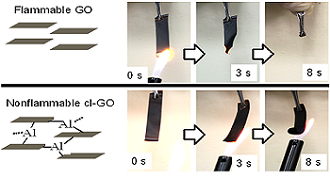
Graphene oxide (GO), a flake-like intermediate for making graphene from graphite, was proven by our lab and others’ to possess a fire hazard that can jeopardize the graphene large-scale production and wide applications. To solve this longstanding built-in problem, we have developed a simple, facile and scalable method for polymerizing the irregularly shaped/sized graphene oxide flakes with multivalent metal cations, such as Al3+, into a freestanding, mechanically strong, and paper-like flexible inflammable membrane in the form of a GO-oligomer. Thus-formed membrane that’s transparent to the naked eyes, about 10 um in thickness, resists in-air burning on an open flame (at which non-crosslinked graphene oxide was burnt out within ∼5 seconds), and resist hydrolysis in water over long time (during which non-crosslinked graphene oxide membrane quickly decomposes). Characterization data from SEM, HRTEM, XRD, microRaman, TGA/DSC, FTIR, and flame tests concluded that the multivalent cations effectively cross-linked the GO flakes, which in turn confirmed a strategy for polymerizing sheet-like nanomaterials in general.
With the much improved on-flame and in-water stabilities, the membrane can enable e.g. roll-to-roll printing of high-temperature fuel cell membrane, battery membrane separators and electrodes, wearable electronics, flexible electronics, flexible thin-foil solar-cells, spray-able device packaging, sensors, etc. Other multivalent cations of transition metals and rare earth metals can likewise produce the new polymers with widely tunable electrical, magnetic and optical properties that ordinary graphene cannot possess.
Lunch Break: 13:15 - 13:55 @ Athens
Kartik Ghosh
Missouri State University, USA
Title: Electrical and Magneto Transport Properties of Reduced Graphene Oxide Thin Films
Time : 13:55 - 14:15

Biography:
Kartik Ghosh has completed his PhD from Tata Institute of Fundamental Research and Post-doctoral studies from the University of Maryland at College Park and Argonne National Laboratory. Currently, he is a Professor of Physics and Materials Science at Missouri State University. Over the last 25 years in his research career, he has been developing organic and inorganic thin films, nanomaterials, and their heterostructures for potential applications in the field of Spintronics, Renewable Energy, and Nano Biotechnology and has made important contributions to these fields. He has published over 150 peer-reviewed articles in highly cited journals and has been serving as a reviewer in many reputed journals.
Abstract:
Our goal is to follow a completely novel route to fabricate large area reduced graphene oxide (RGO) thin film using physical vapor deposition technique to achieve high charge carrier mobility with better conductivity. In order to avoid the chemical reagent based reduction path which often uses toxic reducing compound such as N2H4 and NaBH4, we used the pulsed laser deposition (PLD) technique. Large area uniform thin films of RGO were synthesized by PLD. A number of structural properties including the defect density, average size of sp2 clusters and degree of reduction have been investigated by Raman spectroscopy, X-ray photoelectron spectroscopy and x-ray diffraction. Temperature dependent (5K - 350K) four terminal electrical transport property measurements confirms variable range hopping and thermally activated transport mechanism of the charge carriers at low (5K - 210K) and high temperature (210K - 350K) regions, respectively. The calculated localization length, DOS near Fermi level (EF), hopping energy, and Arrhenius energy gap provide significant information to explain excellent electrical properties in the
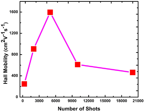
RGO films. Hall mobility measurement confirms p-type characteristics of the thin films. The charge carrier Hall mobility can be engineered by tuning the growth parameters, and the measured maximum mobility was 1596 cm2v-1s-1. The optimization of the improved electrical property is well supported by Raman spectroscopy. The transport properties of RGO samples are dependent on a number of factors including the density of the defect states, size of the sp2 clusters, degree of reduction, and the morphology of the thin film.
Gilbert Chahine
The National Centre for Scientific research, France
Title: Suspended graphene and nanoscrolls explored by nanofocused x-rays
Time : 14:15 - 14:35

Biography:
Gilbert Chahine is a Research-Engineer at the CNRS and working on the BM02 beamline at the European Synchrotron (ESRF) in Grenoble France. After a PhD in Materials Science with the highest distinction degree at the CEA in France, during his Post-doc he developed a new x-ray imaging technique (KMap) along with user-friendly software for the analysis of 5D data sets. This technique is now highly requested by a large community of researchers form international institutes to perform new types of experiments such as in situ and operando strain imaging, with the highest available resolution, of nano devices for photonics, photo voltaics and optoelectronics. Besides coordinating several projects involving international academic and industrial institutions in the field of strained semiconductors, he became interested in adapting the latest advances in synchrotron x-ray sources for a direct model-free in-depth probe of 2D materials’ local structure for a better understanding of their properties.
Abstract:
Structure determination of crystal lattice parameters and orientation with high precision is rather straightforward for bulk 3D-materials. X-ray diffraction proved especially powerful in this respect across the years. On the contrary, structural determination of 2D crystals with the help of x-rays is more demanding. So far, exploiting interferences between a crystalline substrate and graphene, it was possible to accurately determine the lattice parameter of graphene, averaged across the ~1cm2 surface of a sample. Such studies are however restricted to graphene samples of macroscopically uniform crystalline orientation. However most graphene samples of relevance for potential applications (micro-electronics, telecom, displays) exhibit in homogeneities, as they are composed of single-crystal grains (~10µm), each having different crystalline orientation and strain. Finely characterizing such structural features requires probing suspended graphene with the help of nano-shaped beams. Using, electron beams instead of nanofocused x-rays, we managed to conduct simultaneously small and wide angle x-ray scattering (SAXS/WAXS) characterizations with high resolution in reciprocal space and an unprecedented resolution of 200nm in real space, Accordingly we were able to map the structural variations in two- dimensions, revealing in this way strain maps for the suspended few-layer graphene membrane and the morphological features at the edges of the flakes, where it forms scrolls with a typical length of the order of 10µm and a diameter of the order of 10nm. The orientation of the nanoscrolls could for instance be resolved.
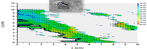
Our complementary analysis with spatially-resolved Raman spectroscopy provides the unique opportunity to unambiguously determine the Grüneisen parameters of graphene, linking the deformation to the energy of its vibration modes, without any particular assumption. These experiments pave the way to advance in-situ experiments and for exploring 2D crystals and their phase transitions using synchrotron radiation especially with the future upgrade programs in the European Synchrotron for outstanding expected brilliance.
Richard Clark
Morgan Advanced Materials, USA
Title: Graphene manufacture and simultaneous functionalization by electrochemical exfoliation – a winning paradigm or just another mark on an overpopulated IP map?
Time : 14:35 - 14:55

Biography:
Richard A Clark works at Morgan Advanced Materials (LSE: MGAM), is a UK-headquartered global manufacturer of specialized engineered products made from carbon, advanced ceramics and composites. After being educated as a Chemical Engineer, he has been with Morgan for 30 years, developing and commercializing materials across the spectrum of Morgan’s portfolio, most recently focusing on materials related to energy. He was part of Morgan’s team engaged with the University of Cambridge developing electrolytically produced carbon nanomaterials and has continued his involvement in this field in collaboration with Morgan’s team at the Manchester NGI.
Abstract:
Since the groundbreaking article in Science in October 2004 describing the occurrence, isolation and potential significance of graphene, there has been a huge interest in developing industrially scalable methods of manufacture from bottom-up and top-down routes. By mid-2015 the number of international patent applications had already exceeded 10,000 and the annual rate was continuing to accelerate exponentially. Over 11,000 scientific papers (more than one per hour) with graphene in the title were published in 2015. Hundreds of millions of dollars are being invested in such programs as Europe’s graphene flagship consortium as well in in many other academic and commercial organizations globally, although this far exceeds the current annual revenue of graphene producers, by an order of magnitude or more. One such top-down route developed for the mass manufacture of graphene involves electrochemical exfoliation. Promising in its own right, this can be performed using diazonium salts at a single applied potential, simultaneously functionalizing the single- or few-layer graphene generated. Not only does this remove the need for the secondary processing step, it is also a particularly effective means of separating the functionalized layers by virtue of the nitrogen generated during the in-situ diazonium reduction. Most typically for other top-down methods for production of graphene, functionalization is considered a separate, but necessary operation to permit dispersion, so this method appears to offer some clear economic advantages.
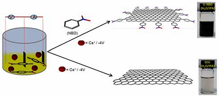
Although the method applies to a plurality of diazonium salts, nitrobenzenediazonium (NBD) salts are particularly effective as demonstrated by quantitative assessment of dispersibility and efficacy in improving capacitance at the laboratory scale. This presentation will review the current status of the graphene industry and specifically review the recent progress on electrochemical exfoliation in this context.
Guang Li
Donghua University, China
Title: The control of pore sizes in porous carbon fiber and its enhanced microwave absorption
Time : 14:55 - 15:15

Biography:
Guang Li has received her MSc degree in Chemistry from China Textile University in 1985 and PhD in Material Science and Engineering from Donghua University in 2006, respectively. She has worked as an Assistant Professor, a Lecturer and an Associate Professor at China Textile University from 1986 to 1999. She was a Senior Visiting Scholar in the University of Twente (Netherlands). She was promoted to be a full Professor at Donghua University (China) in 1999, and is continuously working on high performance polymer synthesis, porous carbon fibers and their associated processing for energy applications including PEM fuel cells. She has led more than 20 projects supported by Chinese National Natural Science Foundation, Ministry of Education of China, Shanghai Municipal Science and Technology Commission, etc. She has published more than 100 scientific papers in high-impacting peer-reviewed journals. She has given more than 24 keynote/invited/oral presentations in international conferences, co-authored 4 books and owns 26 patents. She has been awarded several prizes for recognizing her great contributions to science and technology, including the second prize of Science and Technology Progress in Shanghai, the second prize from Ministry of Education of China, the second prize from China Textile Industry Association, etc.
Abstract:
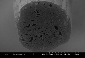
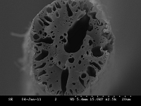
As one of the carbon materials, the porous carbon fiber has played a great role as catalyst support, separation by absorption; gas storage etc. based on its high aspect ratio. Among related publications, few studies focused on the microwave absorption characteristics of porous carbon fibers, although a great number of papers concerned carbon materials such as carbon black, fiber, tube as microwave absorbents. In this study, porous carbon fibers were prepared through carbonization of the blend fibers composed of poly (acrylonitrile) (PAN) and poly (methyl methacrylate) (PMMA) with 70 wt % of PAN. The pore size in porous carbon fibers could be controlled by changing the average molecular weight of PAN. The pores of 1-10μm and 0.1-1μm in diameter were obtained from the blend fibers where the average molecular weight of PAN is 51000 and 83000 g/mol, respectively (Figure 1). The obtained porous carbon fibers were used as absorbents to make epoxy composites with addition of 2-6 wt%. The microwave absorption properties were stimulated based on a model for a single-layer plane wave absorber. The results explained the porous carbon fiber showed much better microwave absorption than carbon nanofiber, and the porous carbon fiber with small size of pores showed much better microwave absorption than that with large size of pores, as shown in figure 2.
It is believed that the enhanced microwave absorption from the porous carbon fibers is due to a combination of the dielectric-type absorption and the interference of multi-reflected microwaves. When the pore size in porous carbon fibers is large, the air-absorber interfaces could be reduced at the same pore volume. Therefore, the superior microwave absorption of composites filled by porous carbon fiber with smaller pore size may be ascribed to the combination of absorption and interference of microwaves.
Steve Park
Korea Advanced Institute of Science and technology, South Korea
Title: The solution-based sorting and assembly of single-walled carbon nanotubes for transistors and pressure sensors
Time : 15:15 - 15:35

Biography:
Prof. Steve Park received his dual Bachelor’s degree in materials science and engineering and physics with magna cum laude from the University of Illinois at Urbana-Champaign and Knox College. He then worked as a technical staff for NanoInk Inc., developing commercial applications of dip-pen nanolithography. Prof. Park then received his Master of Science and Ph D from Stanford University in Materials Science and Engineering under the Prof. Zhenan Bao, researching on carbon nanotube and organic-based electronics. He then conducted his postdoctoral work at Columbia University in the electrical engineering and biomedical engineering department, working on piezoelectric polymer-based implantable devices
Abstract:
Single-walled carbon nanotubes (SWNTs) are an ideal channel material for next generation sub-10 nm gate-length transistors due to their ultra-thin body and high carrier transport properties. In addition, due to their high mechanical flexibility, SWNTs are an ideal candidate for flexible and stretchable sensors and electronics [1]. To use SWNTs as channel material in transistors, 1) semiconducting SWNTs must be fully separated from metallic SWNTs and 2) densely aligned over a large area, in a facile and scalable manner. To address the former, we have investigated solution-based sorting of SWNTs using various conjugated polymers.
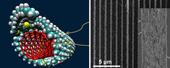
[2] With proper design of conjugated polymers, certain diameter range of the semiconducting SWNTs was selectively dispersed with high efficiency.[3] To address the latter, we have developed solution-shearing technique to densely align SWNTs over a large area, with density as high as 200 SWNTs/μm.[4] On-current density was improved by an order of magnitude over that of random network; however, with higher packing density, loss of electrostatic control was evident. These observations shed light on the behavior of aligned SWNT films and suggest possible approaches to further improve the electrical properties of SWNT-based transistors. We have also developed a stretchable capacitive tactile sensor based on carbon nanotube electrodes.[5] By buckling the carbon nanotubes into 'nanosprings,' high degree of stretchability up to 100% was attained. As the dielectric layer, we have implemented an air gap and a porous PDMS layer. The air gap enabled high sensitivity of 0.7 kPa^-1 in the low pressure regime (<1 kPa), while the porous PDMS layer enabled better pressure sensitivity in the tens of kPa regime. In addition, by simultaneously detecting the change in capacitance and the resistance of the top and bottom electrodes, various tactile inputs such as normal pressure, bending, and lateral strain was differentiated.
Coffee Break: 15:40 - 16:00 @ Foyer
- Graphene synthesis | Electrochemistry of diamond and nano carbon materials
Location: Zurich

Chair
Somnath Bhattacharya
University of Witwatersrand, South Africa

Co-Chair
Irina V Antonova
Institute of Semiconductor physics, Russia
Session Introduction
Irina V Antonova
Institute of Semiconductor Physics, Russia
Title: Graphene/fluorinated graphene systems for a wide spectrum of applications
Time : 16:00 - 16:20

Biography:
Irina V Antonova graduated from Department of Physics and Engineering, Novosibirsk State Technical University in 1979. Since 1981, she has been working in the Institute of Semiconductor Physics, Siberian Branch of the Russian Academy of Science. Presently, she occupies a leading Researcher Position at the Institute of Semiconductor Physics and heads a group of researchers who deal with investigation of graphene and its derivatives. Her activity was connected with transport and recharging phenomena in nanocomposite layers (Si, Ge nanocrystals in dielectric matrix), and localized states in heterostructures (SOI, quantum wells and quantum dots), high-pressure-related effects and surface passivation phenomena. The scope of her current research includes chemical functionalization of graphene, fabrication of graphene-based heterostructures and arrays of graphene quantum dots embedded in a fluorographene matrix, transport and recharging phenomena in nanocomposite layers. She has above 240 papers.
Abstract:
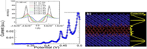
In the report we consider the properties of partially fluorinated graphene (FG) created with the use of a simple fluorination method based on the treatment in an aqueous solution of hydrofluoric acid. FG films can be formed from CVD grown graphene and a graphene suspension. A possibility to control a size of graphene flakes in a suspension in the course of their fluorination was also demonstrated. The possibility to create the FG films with arrays of graphene quantum dots (GQDs) is revealed. The spectrum of quantum confinement levels for GQDs in a fluorinated matrix and a charge relaxation time from GQDs are determined with the use of charge transient deep level spectroscopy. The time of GQD recharging can be controlled by means of GQD thickness variation or daylight assistance. This finding makes films with GQDs promising for flash memory applications. Fluorination of domain boundaries leads to a strong current modulation by gate voltage with an ON/OFF relation ~105 (the property important for field-effect transistors). The negative differential resistance (NDR) and a step-like increase in the current are found for films created from the fluorinated graphene suspension. The NDR resulting from the formation of a potential barrier system in the film is observed for a relatively low fluorination degree.
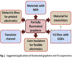
The observation of NDR in FG films widens the range of possible applications. A stable resistive switching effect is detected in films created from the FG suspension. The origin of resistive switching was found to connect with the appearance of traps with energy 0.08 eV and the recharging time lower than 700 ns. The charges in metal–insulator–semiconductor structures with FG dielectric layer have been estimated as the ultra-low values of (0.5–2) x1010 cm-2. Suspensions of fluorinated graphene with nanometer size flakes are of interest for the development of 2D ink-jet printing technologies and the production of thermally and chemically stable dielectric films for nanoelectronics on rigid and flexible substrates.
Omotayo A Arotiba
University of Johannesburg, South Africa
Title: The application of Diamond, Graphene and Exfoliated graphite in electrochemical sensing and electrochemical degradation of organic pollutants in water
Time : 16:20-16:40

Biography:
Omotayo A. Arotiba is an Electrochemist with expertise in the applications of nanomaterials such as carbons, dendrimers, metal/metal oxides for the development of (bio)sensors and photo-electrochemical systems for biomedical, environmental (water) related problems. He is currently involved in the development of electrochemical water treatment technologies as well as sensors for toxic metals, toxins and many substances of biomedical importance. He received his BSc (Hons) and MSc in Industrial Chemistry from the University of Ilorin and the University of Benin both in Nigeria. He obtained his PhD (in 2009) from the Department of Chemistry, University of the Western Cape, South Africa. He joined the Department of Applied Chemistry, University of Johannesburg in 2010 where he is currently a Professor. He is a member of the International Society of Electrochemistry, Royal Society of Chemistry and South African Chemical institute
Abstract:
This work presents an overview of our research on the use of carbon – diamond, graphene and exfoliated graphite – in the development of electrochemical sensors and photoanodic electrodes for the electrochemical degradation of organic water pollutants. In electrochemical sensing, a novel ternary composite electrode from diamond, graphene and polyaniline was prepared, characterised and applied for the electrochemical determination of 2,4-dichlorophenol (2,4-DCP) in aqueous media. The composite, obtained via the oxidative polymerisation of aniline in the presence of graphene and diamond, was characterised by FTIR spectroscopy, Raman spectroscopy etc and used to modify a glassy carbon electrode. The electrochemical properties of the bare and modified electrodes were investigated using cyclic voltammetry, square wave voltammetry (SWV) and impedance. The determination of 2,4-DCP in 0.1 M HNO3 was carried out using SWV and a detection limit of 0.25 μM was calculated.
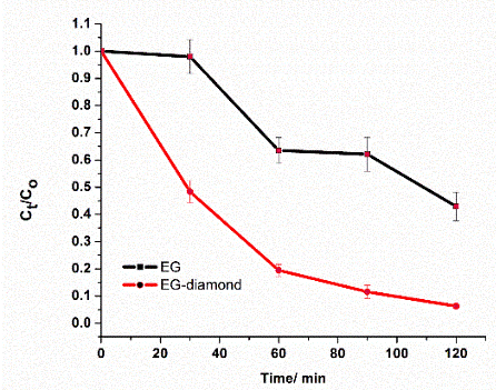
The electrode exhibited antifouling capabilities during the electro-oxidation of 2,4-DCP. For electrochemical degradation, composites electrode consisting of exfoliated graphite (EG) and diamond were prepared and used for the electrochemical degradation of organics in water. The extent of degradation of the organics was monitored with UV/VIS spectroscopy and total organic carbon. Results showed that the incorporation of diamond into EG yielded a more robust electrode in terms of current density and also enhanced the rate of degradation of the organics. This approach is promising for the development of alternative or complementary methods for water treatment
Karin Larrson
Uppsala University, Sweden
Title: Electronic Properties of Various B-doped Diamond(111)// Dye Molecule Interfaces
Time : 16:40 - 17:00

Biography:
Karin Larsson is a Professor in Inorganic Chemistry at the Department of Materials Chemistry, Uppsala University, Sweden. She is the leader of the Theoretical Materials Chemistry Group at the Department of Materials Chemistry. The scientific focus is on interpretation, understanding and prediction of the following processes/properties for both solid/gas interfaces, as well as for solid/liquid interfaces; i) CVD growth (incl. doping and its effect on surface properties), iii) interfacial processes for renewable energy applications (e.g. electrochemical processes), and iv) interfacial processes for e.g. bone regeneration (incl. biofunctionalisation of surfaces).
Abstract:
Diamond is a widely known material for its many excellent properties. A B-doped diamond is an excellent p-type material for solar cell usage. Due to some specific properties (e.g., large chemical inertness, very high carrier mobility for both electron and holes), it is considered as one of the strongest candidates for photovoltic electric generation. However, in order to implement the usage of diamond in solar energy applications, properties like the i) electrochemical window, ii) possibility for interfacial charge transfer, and iii) stability of functionalized surface, have to be further studied and optimized.
In the present investigation, the adsorption of different dye molecules onto H-terminated diamond (111) surfaces, have been theoretically studied using Density Functional Theory (DFT) calculations. The diamond surfaces were B-doped in order to make them p-type semi-conducting. The choice of dyes was based on the match between the electronic structures of these H-terminated B-doped diamond surfaces, and the respective dye molecules. The dye molecules in the present study included C20H13NO3S4 (A), C35H37NO2S3 (B), C34H38OS2(C), C32H36OS2(D), and C31H35S3Br(E). These dyes differ in the various functional groups, which have the role as electron acceptors. The main goal with the present study was thereby to investigate and compare the photovoltaic efficiency of the various dyes when attached to B-doped and H-terminated diamond (111) surfaces.
The calculated absortion spectra for in principle all of the different dyes were shown to be located in the most intense part of the sunlight spectrum.

Biography:
James C Sung was responsible for diamond production technology at GE Super Abrasives, for diamond tools development at Norton. He has set the diamond grid specifications for diamond disks used worldwide for CMP of IC wafers, and helped IPO of Kink Company in Taiwan. He co-founded graphene synthetic with Huang-He worldwide, the world's largest diamond maker located in Henan China. He is currently, the Chairman of Applied Diamond Inc., selling the most advanced CMP diamond disks-V the manufacture of next generation interconnects.
Abstract:
Graphene is the stretched diamond (111) plane graphene can be formed martensitic alloy without breaking the carbon bonds, on diamond surface by specialty heat treatment in vacuum. In this case graphene on diamond (GOD) hetero-epitaxy is similar to homo-epitaxy so the signal transmission is continuous. GOD is an ideal computational device as graphene contains the most effective transmission lattice, capable of terahertz communication by Mach 100 speed of phonon (lattice vibration). On the other hand, diamond is considered to be the most stable quantum computing solid due to its highest Debye temperature. During the quantum computing, the Q-bits must be entangled without atomic vibration, and diamond’s super hard lattice is capable to maintain this stability for milliseconds, even at room temperature. Diamond contains about 1% C13 isotope atoms in the lattice. These atoms may be ion planted and heat treated to cluster as Q-bits.
The superposition of spins from the extra neutron in the nuclei would be the best mechanism for quantum computing. With about 50 Q-bits entangled in milliseconds while these Q-bits are stationary, the vast computational possibilities can tackle even more difficult problems that for all human transistors combined. With GOD, the quantum computing can be initiated with graphene on cubical face (100) of diamond; and the collapsed quantum waves may exit from octahedral face (111). Thus, GOD would be the dream AI chip that outperforms even the smartest combinations of all current computers interconnected together.
Pralay Gayen
University of Illinois at Chicago, USA
Title: ¬¬¬Fluorination of Boron-doped Diamond Film Electrodes for Minimization of Perchlorate Formation
Time : 17:20 - 17:40

Biography:
Pralay Gayen has expertise in the area of electrochemical treatment of water and wastewater matrix. His research objective is to develop effective, highly robust and highly selective material to detect antibiotics, degrade different organics and inhibit perchlorate formation in water matrix as all these compounds pose serious health hazard. He has been using boron-doped diamond (BDD) electrodes for wastewater treatment as they are efficient at oxidizing recalcitrant organic compounds through electrochemical oxidation. He has also been using differently fluorinated BDD electrodes to prevent perchlorate formation without affecting organic oxidation as perchlorate is carcinogenic and formed through electrochemical oxidation of chloride. He also fabricated a sensor comprising BDD electrodes modified by carbon nanotube and nafion for the electrochemical detection of antibiotic (ciprofloxacin) in water and wastewater matrix as the presence of antibiotics for a long time will cause potential emergence of drug resistant bacteria.
Abstract:
The effects of surface fluorination on perchlorate formation rates as well as organic compound oxidation (phenol, terephthalic acid (TA)) rates at boron-doped diamond (BDD) film anodes were investigated. Different fluorination methods like electrochemical oxidation of perfluorooctanoic acid (PFOA) solutions, radio frequency plasma with H2/CF4 gas, and silanization with aliphatic (1H,1H,2H,2H perfluorodecyltrichlorosilane) and aromatic (triethoxy(pentafluorophenyl)silane) compounds have been used to incorporate fluorinated functional groups on the BDD surface, which was confirmed by X-ray photoelectron spectroscopy. The perchlorate formation rate was lowered by only 63.2% for PFOA modified BDD electrode and remained similar for both the plasma fluorinated and aromatic silanized BDD electrodes. However the perchlorate formation rate (<0.12 µmoles m-2 min-1) via chlorate and chloride oxidation was lowered by 99.96% and 99.95%, respectively, for aliphatic silanized electrode. The phenol oxidation rate decreased by 61% and 16.3% (with chloride) and TA oxidation decreased by 55% for the aliphatic silanized electrode. The apparent selectivity of the aliphatic silanized BDD electrode increased by 2.1-fold and 2.2-fold for TA and phenol, respectively whereas it decreased 680-fold for perchlorate formation. Fe(CN)63-/4- and Fe3+/2+ redox
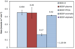
couples using cyclic voltammetry indicated that steric hindrance and hydrophobic effects between the fluorinated chains and chlorate ions may be responsible for the very low perchlorate formation on the aliphatic silanized (< 0.12 µmoles m-2 min-1) and PFOA modified electrodes (0.17 mmoles m-2 min-1). The PFOA modified BDD electrode showed a similar perchlorate formation rate after ageing, which confirmed high stability of the PFOA modification. The perchlorate formation rate was below the detection limit (<0.12 µmoles m-2 min-1) for up to 10 consecutive chlorate oxidation experiments and showed almost 90% decrease in perchlorate formation thereafter, which confirmed very high stability of aliphatic silanization under OHŸ production.
Marc Cretin
Université de Montpellier, France
Title: Carbon based materials: a promising approach for water depollution by electrochemical advanced oxidation processes
Time : 17:40 - 18:00

Biography:
Marc Cretin was born in France, in 1969. He received his Ph.D. degree in Electrochemistry (National Polytechnic
Institute of Grenoble France) in 1996 and joined Geneva University to develop electrochemical sensors for biomedical and environmental analysis. In 1998 he gained a position of assistant professor (ENSCM/Montpellier/France) to work on membranes materials for detection, separation and reaction. He’s full professor since 2012 at the University of Montpellier and works mainly in the field of materials for energ y and environment. He focuses his research mainly on electroactive materials for fuel cells, biofuel cells, EAOP (electrochemical advanced oxidation processes) and ceramic membranes for water treatment. He’s currently Director of the department “Physico-Chemistry, Interface and Polymer” at the European Membrane Institute of Montpellier (IEM) and co-director of the International French-Russia Laboratory MEIPA “Ion Exchange Membranes and Associated Processes”. Up to March 2017, he has co-authored more than 80 peer reviewed papers
Abstract:
Scarcity of pure water worldwide is dramatically affecting the economic development of Third Countries but also the industrial growth of others. Towards the water recycling and reuse, Electrochemical Advanced Oxidation Processes (EAOPs) are of high interest since they are very efficient in the degradation of refractory pollutants that cannot be eliminated by conventional techniques. Amongst them, the electro-Fenton (EF) process allows the in situ generation of highly reactive and nonselective hydroxyl radicals indirectly by cathodic oxygen reduction, its subsequent H2O2 production and further Fenton reaction (eq. 1).
Fe2+ + H2O2 + H+ → Fe3+ + •OH + H2O (eq. 1)
Carbon felt is a good candidate to produce H2O2 from the reduction of dissolved oxygen [1] but it suffers from drawbacks like relatively low electronic conductivity and electrochemical active surface area. With the aim to increase carbon felt efficiency toward the electro-Fenton process, we develop in our research team, different modification routes to get microporous reactive carbon-based structures. It deals from basic thermal treatment under controlled atmosphere [2] to microporous carboneous coating prepared by combining Atomic Layer Deposition and solvothermal MOF growth on carbon felt [3], going through graphene functionalization [4] and LDH deposition for heterogeneous catalysis [5]. We will discuss synthesis, characterization and electrocatalytic properties of the different structures. Carbon based materials will be then integrated in a electrolysis system for water treatment but also in a prospective fuel cell – Fenton system for zero-energy water depollution [3]. Efficiency will be shown through the degradation and mineralization of pharmaceutical residues and organic dyes.
End of Day 1